- Forums
- Product Forums
- General Purpose MicrocontrollersGeneral Purpose Microcontrollers
- i.MX Forumsi.MX Forums
- QorIQ Processing PlatformsQorIQ Processing Platforms
- Identification and SecurityIdentification and Security
- Power ManagementPower Management
- Wireless ConnectivityWireless Connectivity
- RFID / NFCRFID / NFC
- Advanced AnalogAdvanced Analog
- MCX Microcontrollers
- S32G
- S32K
- S32V
- MPC5xxx
- Other NXP Products
- S12 / MagniV Microcontrollers
- Powertrain and Electrification Analog Drivers
- Sensors
- Vybrid Processors
- Digital Signal Controllers
- 8-bit Microcontrollers
- ColdFire/68K Microcontrollers and Processors
- PowerQUICC Processors
- OSBDM and TBDML
- S32M
- S32Z/E
-
- Solution Forums
- Software Forums
- MCUXpresso Software and ToolsMCUXpresso Software and Tools
- CodeWarriorCodeWarrior
- MQX Software SolutionsMQX Software Solutions
- Model-Based Design Toolbox (MBDT)Model-Based Design Toolbox (MBDT)
- FreeMASTER
- eIQ Machine Learning Software
- Embedded Software and Tools Clinic
- S32 SDK
- S32 Design Studio
- GUI Guider
- Zephyr Project
- Voice Technology
- Application Software Packs
- Secure Provisioning SDK (SPSDK)
- Processor Expert Software
- Generative AI & LLMs
-
- Topics
- Mobile Robotics - Drones and RoversMobile Robotics - Drones and Rovers
- NXP Training ContentNXP Training Content
- University ProgramsUniversity Programs
- Rapid IoT
- NXP Designs
- SafeAssure-Community
- OSS Security & Maintenance
- Using Our Community
-
- Cloud Lab Forums
-
- Knowledge Bases
- ARM Microcontrollers
- i.MX Processors
- Identification and Security
- Model-Based Design Toolbox (MBDT)
- QorIQ Processing Platforms
- S32 Automotive Processing Platform
- Wireless Connectivity
- CodeWarrior
- MCUXpresso Suite of Software and Tools
- MQX Software Solutions
- RFID / NFC
- Advanced Analog
-
- NXP Tech Blogs
- Home
- :
- General Purpose Microcontrollers
- :
- LPC Microcontrollers
- :
- LPC5528 USB1 Double Buffer Design
LPC5528 USB1 Double Buffer Design
- Subscribe to RSS Feed
- Mark Topic as New
- Mark Topic as Read
- Float this Topic for Current User
- Bookmark
- Subscribe
- Mute
- Printer Friendly Page
- Mark as New
- Bookmark
- Subscribe
- Mute
- Subscribe to RSS Feed
- Permalink
- Report Inappropriate Content
Hi all,
Based on the USB sample code dev_hid_generic_bm, we can see that the SDK enables double buffer by default. After studying for days, I found that this sample code uses producerOdd and consumerOdd to toggle the USB RAM buffer. But these flags are not HW registers.
My questions are:
1. How can I find out which one is the latest USB buffer in the USB RAM using the USB1 register (if the host sends two endpoint out to the same physical EP)? Can the EPTOGGLE register (Table 844) or the EPINUSE register(Table 839) help me to know which is the latest USB buffer in USB RAM if USB double buffer is full?
2. Is there a way that I can make USB double buffer fully filled?
Thanks.
BR,
Peter
Solved! Go to Solution.
- Mark as New
- Bookmark
- Subscribe
- Mute
- Subscribe to RSS Feed
- Permalink
- Report Inappropriate Content
Hi,
I suppose that there is not dedicated doc which focuses on the USB double buffer design.
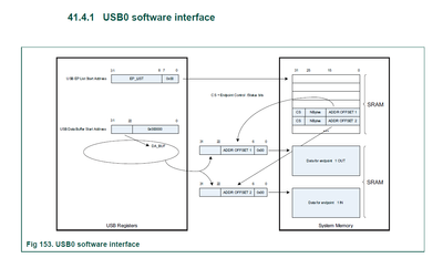
This is the USB buffer architecture:
For the double buffer design, for each logic endpoints, for the input buffer, there are two buffer for each ENDPOINT IN, for out buffer, there are two buffers.
So each logic end points will like:
IN buffer for each logic endpoint.
CS NBYTES Offset1
CS NBYTES Offset2
OUT buffer for each logic endpoint.
CS NBYTES Offset3
CS NBYTES Offset4
Hope it can help you
BR
XiangJun Rong
- Mark as New
- Bookmark
- Subscribe
- Mute
- Subscribe to RSS Feed
- Permalink
- Report Inappropriate Content
Hi XiangJun,
Do you have a document that explains the detailed double buffer design? I know double buffer can enhance the USB transfer efficiency but I'm not sure how it works.
As we know, once the active bit is cleared by the HW, it will trigger the USB interrupt and let us know which EP has the data coming in or out. Meanwhile, the HW will toggle the EPINUSE to get ready for the next same EP data transfer. My guess is that once it triggers the USB interrupt, the HW is ready for the next data. Am I correct?
Thanks.
BR,
Peter
- Mark as New
- Bookmark
- Subscribe
- Mute
- Subscribe to RSS Feed
- Permalink
- Report Inappropriate Content
Hi,
This is the AE team reply:
"How can I find out which one is the latest USB buffer in the USB RAM using the USB1 register (if the host sends two endpoint out to the same physical EP)? Can the EPTOGGLE register (Table 844) or the EPINUSE register(Table 839) help me to know which is the latest USB buffer in USB RAM if USB double buffer is full?
User can use "USB EP Buffer in use" detect which buffer in use
2. Is there a way that I can make USB double buffer fully filled?
set the max transfer size in descriptor, and make sure the HOST side can reach the max transfer size.
"
BR
XiangJun Rong

