
- Forums
- Product Forums
- General Purpose MicrocontrollersGeneral Purpose Microcontrollers
- i.MX Forumsi.MX Forums
- QorIQ Processing PlatformsQorIQ Processing Platforms
- Identification and SecurityIdentification and Security
- Power ManagementPower Management
- Wireless ConnectivityWireless Connectivity
- RFID / NFCRFID / NFC
- Advanced AnalogAdvanced Analog
- Neural Processing UnitsNeural Processing Units
- MCX Microcontrollers
- S32G
- S32K
- S32V
- MPC5xxx
- Other NXP Products
- S12 / MagniV Microcontrollers
- Powertrain and Electrification Analog Drivers
- Sensors
- Vybrid Processors
- Digital Signal Controllers
- 8-bit Microcontrollers
- ColdFire/68K Microcontrollers and Processors
- PowerQUICC Processors
- OSBDM and TBDML
- S32M
- S32Z/E
-
- Solution Forums
- Software Forums
- MCUXpresso Software and ToolsMCUXpresso Software and Tools
- CodeWarriorCodeWarrior
- MQX Software SolutionsMQX Software Solutions
- Model-Based Design Toolbox (MBDT)Model-Based Design Toolbox (MBDT)
- FreeMASTER
- eIQ Machine Learning Software
- Embedded Software and Tools Clinic
- S32 SDK
- S32 Design Studio
- GUI Guider
- Zephyr Project
- Voice Technology
- Application Software Packs
- Secure Provisioning SDK (SPSDK)
- Processor Expert Software
- Generative AI & LLMs
-
- Topics
- Mobile Robotics - Drones and RoversMobile Robotics - Drones and Rovers
- NXP Training ContentNXP Training Content
- University ProgramsUniversity Programs
- Rapid IoT
- NXP Designs
- SafeAssure-Community
- OSS Security & Maintenance
- Using Our Community
-
- Cloud Lab Forums
-
- Knowledge Bases
- ARM Microcontrollers
- i.MX Processors
- Identification and Security
- Model-Based Design Toolbox (MBDT)
- QorIQ Processing Platforms
- S32 Automotive Processing Platform
- Wireless Connectivity
- CodeWarrior
- MCUXpresso Suite of Software and Tools
- MQX Software Solutions
- RFID / NFC
- Advanced Analog
- Neural Processing Units
-
- NXP Tech Blogs
- Home
- :
- General Purpose Microcontrollers
- :
- Kinetis Microcontrollers
- :
- K60 RTC VBAT Current Draw
K60 RTC VBAT Current Draw
- Subscribe to RSS Feed
- Mark Topic as New
- Mark Topic as Read
- Float this Topic for Current User
- Bookmark
- Subscribe
- Mute
- Printer Friendly Page
K60 RTC VBAT Current Draw
- Mark as New
- Bookmark
- Subscribe
- Mute
- Subscribe to RSS Feed
- Permalink
- Report Inappropriate Content
I am designing with a MK66FN2M0VMD18 microcontroller and using the RTC circuitry with VBAT power supplied through an external Supercap. I have an external 32.768Khz crystal oscillator for the RTC which uses the internal tunable capacitors configurable by software.
The RTC is configured to use the RTC Alarm output (RTC_WAKEUP_B) to turn on the power supply (required function if power supply is present) and the RTC_CLKOUT pin is also enabled to output the 32.768Khz clock (optional used to monitor/test).
VBAT is powered to approximately 3.0V through diode from 3.3VCC when power is active.
Design intent to is have RTC maintain time when power is OFF for up to 72 hours over operating temp of -40C to +85C.
I looked at the Data sheet and User Guide to try to understand the current draw specifications and would like the current draw clarified.
In Section 2.2.4 Power Mode Transition Operating Behaviors Table 6, it states that IRTC (typ) current draw varies from 357-810 nA -40C to 105C) in VLLS1 mode.
In Section 2.2.5 Power Consumption Operating Behaviors Table 7, it states IDD_VBAT (avg) when CPU is not accessing RTC registers is 6.33uA (at 105C) to 0.8uA (from -40C to 25C) for VBAT = 3.0V.
From description it is not clear to me what the VBAT current draw is when the micro is otherwise unpowered in order to size the appropriate backup power source (supercap) for 72 hour backup.
My questions are:
1. What is worst case IDD_VBAT when VCC is 0V (-40C to +85C)?
2. Does use of RTC_WAKEUP or RTC_CLKOUT affect the IDD_VBAT current draw when VCC = 0V?
3. Do any RTC resister settings affect the current draw of module when VCC = 0?
Thank you.
- Mark as New
- Bookmark
- Subscribe
- Mute
- Subscribe to RSS Feed
- Permalink
- Report Inappropriate Content
I've looked thru the K66 datasheet and also AN4503_Kinetis Power Management app note on behalf of my customer (Dan Waser), and determined that the values Dan is seeking are not specified in either.
The app note and datasheet only mention that the IDD_VBAT value can increase when the VBAT registers are being accessed by the CPU, but does not mention any other potential adders, such as when using RTC_CLKOUT or RTC_WAKEUP. So it appears these do not cause an increase in IDD_VBAT and its fairly isolated from the main power supply, but confirmation would help Dan greatly.
Bottom line, Dan would like to power his product for 72 hours using a SuperCap, and clarifying the worse case IDD_VBAT value and any potential adders will help him pick the correct SuperCap value to enable this.
Thanks,
Gordy Carlson
- Mark as New
- Bookmark
- Subscribe
- Mute
- Subscribe to RSS Feed
- Permalink
- Report Inappropriate Content
Hi Dan and Gordy,
I think there are a few misunderstandings about the RTC and VBAT that are muddying the waters here. I'd like to start with a bit of information...
The RTC_CLKOUT pin is actually in the main VDD domain, the pin is NOT in the VBAT domain. So you should know that RTC_CLKOUT will not toggle if the main VDD =0. RTC_CLKOUT also goes away in some of the low power modes. Because RTC_CLKOUT is in the digital domain, enabling that pin function doesn't affect VBAT current draw (although enabling the oscillator and the RTC itself does as that is all in the VBAT domain).
Also the VBAT domain is a completely isolated domain. There isn't any internal switching so that VBAT is powered from the main when it is available, so for a given RTC configuration and temp VBAT current draw should be fairly stable and doesn't vary based on what is happening with VDD or the power mode of the CPU. The exception is when the core is accessing RTC registers as that generates activity in the VBAT domain.
To answer your questions now...
1. The second set of IDD_VBAT specs in Table 7 are what you want. This is with the RTC and 32kHz osc enabled which sounds like the configuration you will be using. You can't access the registers using the CPU if VDD=0, so this spec covers the VDD=0 case.
2. Not much. As I described above, RTC_CLKOUT is not in the VBAT domain, so it doesn't affect current draw. RTC_WAKEUP is an active low, open drain pin so it won't cause the normal state current to go up if enabled. You'll get a slight bump when the pin asserts based on the pullup resistor value and loading on the pin.
3. I'm not quite sure how to answer this one. If you don't have the RTC enabled, then that would definitely decrease current, but you want to use it, so I don't think that is what you are asking. I guess I can say that the current draw when VDD is powered shouldn't be different than when VDD=0.
Hope this helps,
Melissa
- Mark as New
- Bookmark
- Subscribe
- Mute
- Subscribe to RSS Feed
- Permalink
- Report Inappropriate Content
Melissa,
Dan asks for clarification on what the IDD_Vbat is.... here is a cut/paste of the email response he provided me...
My take on this is that 810na I_RTC value is an adder to the main rail power consumption when the RTC is enabled, and that IDD_Vbat of 0.8ua to 6.33ua over temp is the correct answer. Confirmation appreciated. Thanks!
" Still not sure what current max draw to expect from IDD_VBAT over temp when VC C =0V.
In Section 2.2.4 Power Mode Transition Operating Behaviors Table 6, it states that IRTC (typ) current draw varies from 357 to 810 nA -40C to 105C) in VLLS1 mode.
In Section 2.2.5 Power Consumption Operating Behaviors Table 7, it states IDD_VBAT (avg) when CPU is not accessing RTC registers is 6.33uA (at 105C) to 0.8uA (from -40C to 25C) for VBAT = 3.0V.
Is answer 810nA or 6.33 µA?"
- Mark as New
- Bookmark
- Subscribe
- Mute
- Subscribe to RSS Feed
- Permalink
- Report Inappropriate Content
Hi Gordy,
Table 7 are the specs he wants. You're right, table 6 is an adder on the main supply when the RTC is enabled.
Regards,
Melissa
- Mark as New
- Bookmark
- Subscribe
- Mute
- Subscribe to RSS Feed
- Permalink
- Report Inappropriate Content
Dan is still seeing higher IDD_VBAT than expected, in excess of datasheet specs at high temp....he tested four units for IDD_VBAT with VCC = 0 and is finding current draw greater than the max listed in Table 7 of the data sheet. The control’s circuit was changed to just have resistor between VBAT and VBB pin of K66 to make current draw easier to measure. Voltage was measured across resistor to calculate current. See attachment.
The IC marking is:
MK66FN2M0VMD18
0N65N
CTAD1530E
==================================
Test data over temp with VBB = 1.8V and 3.0V
(Measured values attached as jpg)
I checked the errata for the ON65N mask, there is an errata general power consumption at low temps for "some parts", but nothing noted for issues with IDD_VBAT.
- Mark as New
- Bookmark
- Subscribe
- Mute
- Subscribe to RSS Feed
- Permalink
- Report Inappropriate Content
Hi Gordy,
Are they collecting these numbers on their own hardware? Could I see the schematic? In particular I would like to see how they are connecting the VBAT domain to the main VDD supply (assuming this is what they are doing to charge up the supercap).
Regards,
Melissa
- Mark as New
- Bookmark
- Subscribe
- Mute
- Subscribe to RSS Feed
- Permalink
- Report Inappropriate Content
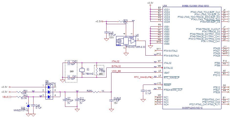
Dan replied to the thread email notification with the below info, ....but just in case, attached is a copy of that part of the schematic along with his description below...
--------------------------------------------
Circuit tested shown below.
D8 pin6 is normally connected to VDD_BB but was removed to eliminate any reverse leakage current error term.
Voltage was measured across R260 to determine IDD_VBAT.
External power supply was placed across C7 to check IDD_VAT at 3.0V and 1.8V.
- 3.3V was power supply was shut down (VCC ≈ 0V).
Unit was otherwise isolated in environmental chamber.
(Note: CU6L6 is ceramic capacitor (low leakage). Removed CU6L6 on one control and verified it had no effect.)
--------------------------------------------------
- Mark as New
- Bookmark
- Subscribe
- Mute
- Subscribe to RSS Feed
- Permalink
- Report Inappropriate Content
Circuit tested shown below.
D8 pin6 is normally connected to VDD_BB but was removed to eliminate any reverse leakage current error term.
Voltage was measured across R260 to determine IDD_VBAT.
External power supply was placed across C7 to check IDD_VAT at 3.0V and 1.8V.
3.3V was power supply was shut down (VCC ≈ 0V).
Unit was otherwise isolated in environmental chamber.
(Note: CU6L6 is ceramic capacitor (low leakage). Removed CU6L6 on one control and verified it had no effect.)
- Mark as New
- Bookmark
- Subscribe
- Mute
- Subscribe to RSS Feed
- Permalink
- Report Inappropriate Content
Hi Dan,
For testing purposes could you try removing D8 from one of the boards. That would completely eliminate the potential for leakage back to the VDD domain.
Thanks,
Melissa
- Mark as New
- Bookmark
- Subscribe
- Mute
- Subscribe to RSS Feed
- Permalink
- Report Inappropriate Content
Thank You Melissa! I suspected RTC_CLKOUT was completely in the VDD domain, great to get a confirmation that it does not impact IDD_VBAT.
regards,
Gordy