- NXP Forums
- Product Forums
- General Purpose MicrocontrollersGeneral Purpose Microcontrollers
- i.MX Forumsi.MX Forums
- QorIQ Processing PlatformsQorIQ Processing Platforms
- Identification and SecurityIdentification and Security
- Power ManagementPower Management
- MCX Microcontrollers
- S32G
- S32K
- S32V
- MPC5xxx
- Other NXP Products
- Wireless Connectivity
- S12 / MagniV Microcontrollers
- Powertrain and Electrification Analog Drivers
- Sensors
- Vybrid Processors
- Digital Signal Controllers
- 8-bit Microcontrollers
- ColdFire/68K Microcontrollers and Processors
- PowerQUICC Processors
- OSBDM and TBDML
-
- Solution Forums
- Software Forums
- MCUXpresso Software and ToolsMCUXpresso Software and Tools
- CodeWarriorCodeWarrior
- MQX Software SolutionsMQX Software Solutions
- Model-Based Design Toolbox (MBDT)Model-Based Design Toolbox (MBDT)
- FreeMASTER
- eIQ Machine Learning Software
- Embedded Software and Tools Clinic
- S32 SDK
- S32 Design Studio
- Vigiles
- GUI Guider
- Zephyr Project
- Voice Technology
- Application Software Packs
- Secure Provisioning SDK (SPSDK)
- Processor Expert Software
-
- Topics
- Mobile Robotics - Drones and RoversMobile Robotics - Drones and Rovers
- NXP Training ContentNXP Training Content
- University ProgramsUniversity Programs
- Rapid IoT
- NXP Designs
- SafeAssure-Community
- OSS Security & Maintenance
- Using Our Community
-
- Cloud Lab Forums
-
- Home
- :
- Model-Based Design Toolbox (MBDT)
- :
- Model-Based Design Toolbox (MBDT)
- :
- Re: PWM Timing and Signal Generation on MKV4xx microprocessors
PWM Timing and Signal Generation on MKV4xx microprocessors
- Subscribe to RSS Feed
- Mark Topic as New
- Mark Topic as Read
- Float this Topic for Current User
- Bookmark
- Subscribe
- Mute
- Printer Friendly Page
PWM Timing and Signal Generation on MKV4xx microprocessors
- Mark as New
- Bookmark
- Subscribe
- Mute
- Subscribe to RSS Feed
- Permalink
- Report Inappropriate Content
this really helps ! Thank you so much so far !
Now I have one question to the timing in the Reference Manual.
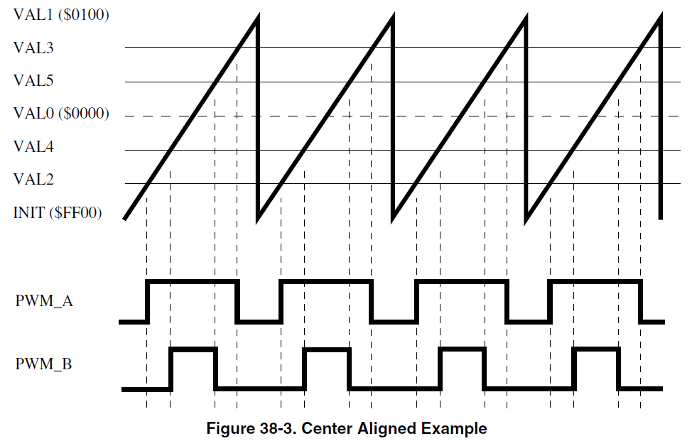
In my opinion one PWM period is from INIT to VAL1.
This would mean that with a duty cycle of 50 percent the on time starts at INIT and ends at VAL0 ?
So for starting the adc conversation at each on time from the PWM I have to set VAL1 ?
Or at which VAL starts the duty cyle ? I think testing this should be possible with the example "kv4xf_eflexpwm_isr" ?
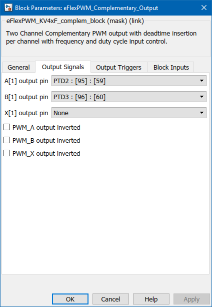
So the PWM_A and PWM_B above are only the timers and not the configured output pins in the block you can see in the picture blow. Is that correct so far ?
- Mark as New
- Bookmark
- Subscribe
- Mute
- Subscribe to RSS Feed
- Permalink
- Report Inappropriate Content
Hello dumitru-daniel.popa
again I have a question for the current sensing.
Like you explained in Module 6: Current Sensing the sensing must be at the time where the Low-Side IGBT is on.
At the moment I trigger the ADC with the PWM command at VAL0 (the middle of PWM_A).
If I'm right the picture shows PWM_A high side IGBT ??
So instead of this I should better trigger the ADC with VAL1, which in complementary PWM mode should be the middle of the on state of the low side IGBT ?
Best regards
Leon
- Mark as New
- Bookmark
- Subscribe
- Mute
- Subscribe to RSS Feed
- Permalink
- Report Inappropriate Content
Hi lethuer2,
In regards with your questions:
In my opinion one PWM period is from INIT to VAL1.
This would mean that with a duty cycle of 50 percent the on time starts at INIT and ends at VAL0 ?
Indeed the PWM Counter starts at INIT and rolls over at VAL1 measuring the one PWM period.
The diagram you are referring to represent the "center aligned" PWM generation when the PWM high and low are aligned in the center to the VAL0.
Your description is valid for edge-aligned PWM generation.
So for starting the adc conversation at each on time from the PWM I have to set VAL1 ?
It depends on with VALx you choose as Output trigger. If you select VAL1 then YES, the ADC conversion will start when FTM counter value = VAL1 (end of PWM period in this particular case)
So the PWM_A and PWM_B above are only the timers and not the configured output pins in the block you can see in the picture blow. Is that correct so far ?
No, that PWM_A and PWM_B are the actual PWM signals that drives the power transitors. PWM_A = A[1] output pin and PWM_B = B[1] output pin.
Hope it helps!
Daniel
- Mark as New
- Bookmark
- Subscribe
- Mute
- Subscribe to RSS Feed
- Permalink
- Report Inappropriate Content
Ok,
if I'm right the image above from the reference Manual is only a example for the generated Output signals and are independant.
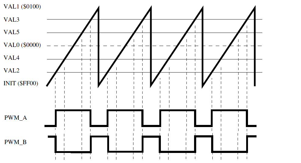
In case of Center aligned and complementary Output the signals from PWM_A and PWM_B would be like this ?
So for starting the ADC conversation with the rising edge of PWM_A I have to choose VAL2 ?
The Options center aligned, edge alligned or assymetrical I can only find in the "Independant PWM output block".
But I want to use the "Complementary eFlexPWM output block" or the "Three-phase eFlexPWM output block".
So what kind of output signal is generated from These two blocks ?
- Mark as New
- Bookmark
- Subscribe
- Mute
- Subscribe to RSS Feed
- Permalink
- Report Inappropriate Content
Hi lethuer2,
Sorry for delay - it seams that i've overlooked your question.
For the Complementary and 3-Phase eFlexPWM blocks the PWM generation mode is hardcoded - "CENTER ALIGNED" type.
As a hint: you can try to build a small demo model, compile it an check the generated code for pwma_sub_module_pwm_param_t structure initialization. All the generated code is based on the Kinetis SDK drivers, therefore you could use SDK documentation as resource.
Hope this helps!
Daniel


