- Forums
- Product Forums
- General Purpose MicrocontrollersGeneral Purpose Microcontrollers
- i.MX Forumsi.MX Forums
- QorIQ Processing PlatformsQorIQ Processing Platforms
- Identification and SecurityIdentification and Security
- Power ManagementPower Management
- MCX Microcontrollers
- S32G
- S32K
- S32V
- MPC5xxx
- Other NXP Products
- Wireless Connectivity
- S12 / MagniV Microcontrollers
- Powertrain and Electrification Analog Drivers
- Sensors
- Vybrid Processors
- Digital Signal Controllers
- 8-bit Microcontrollers
- ColdFire/68K Microcontrollers and Processors
- PowerQUICC Processors
- OSBDM and TBDML
- S32M
-
- Solution Forums
- Software Forums
- MCUXpresso Software and ToolsMCUXpresso Software and Tools
- CodeWarriorCodeWarrior
- MQX Software SolutionsMQX Software Solutions
- Model-Based Design Toolbox (MBDT)Model-Based Design Toolbox (MBDT)
- FreeMASTER
- eIQ Machine Learning Software
- Embedded Software and Tools Clinic
- S32 SDK
- S32 Design Studio
- GUI Guider
- Zephyr Project
- Voice Technology
- Application Software Packs
- Secure Provisioning SDK (SPSDK)
- Processor Expert Software
- MCUXpresso Training Hub
-
- Topics
- Mobile Robotics - Drones and RoversMobile Robotics - Drones and Rovers
- NXP Training ContentNXP Training Content
- University ProgramsUniversity Programs
- Rapid IoT
- NXP Designs
- SafeAssure-Community
- OSS Security & Maintenance
- Using Our Community
-
- Cloud Lab Forums
-
- Knowledge Bases
- ARM Microcontrollers
- i.MX Processors
- Identification and Security
- Model-Based Design Toolbox (MBDT)
- QorIQ Processing Platforms
- S32 Automotive Processing Platform
- Wireless Connectivity
- CodeWarrior
- MCUXpresso Suite of Software and Tools
- MQX Software Solutions
-
- Home
- :
- i.MX フォーラム
- :
- i.MX RT クロスオーバーMCU
- :
- Re: Does I.MXRT1062 LPSPI TCR (Comand Register) require a write to TDR to latch the new command?
Does I.MXRT1062 LPSPI TCR (Comand Register) require a write to TDR to latch the new command?
- RSS フィードを購読する
- トピックを新着としてマーク
- トピックを既読としてマーク
- このトピックを現在のユーザーにフロートします
- ブックマーク
- 購読
- ミュート
- 印刷用ページ
Does I.MXRT1062 LPSPI TCR (Comand Register) require a write to TDR to latch the new command?
- 新着としてマーク
- ブックマーク
- 購読
- ミュート
- RSS フィードを購読する
- ハイライト
- 印刷
- 不適切なコンテンツを報告
Hello,
I am using the I.MXRT1062 and using the LPSPI module. I have to write to a SPI attached LCD display that requires a command pin to be toggled high or low to signify whether the data being written is a command data.
ie.
D/nCmd = 0
Cmd
D/nCmd = 1
Data * n
During this transaction CS has to remain asserted.
I can accomplish this goal by writing to the the TCR 0x78200008, however, when the transaction completes I cannot get TCR 0x78000008 latched into the TCR register.
After writing to TCR do I need to also write to TDR to force a command latch?
- 新着としてマーク
- ブックマーク
- 購読
- ミュート
- RSS フィードを購読する
- ハイライト
- 印刷
- 不適切なコンテンツを報告
- 新着としてマーク
- ブックマーク
- 購読
- ミュート
- RSS フィードを購読する
- ハイライト
- 印刷
- 不適切なコンテンツを報告
I working on MIMXRT1024 to read and write the FRAM(MB85RS4MT). I am able to write the FRAM. After 1st data reading from FRAM, CS pin is not de-assert automatically after clearing TCR[CONT& CONTC & TX].
when i reading FRAM, I writing 4 bytes data FRAM, and i waiting for data by setting LPSPI_TCR_TXMSK_MASK. i am able to read the data. but after reading, TCR[CONT& CONTC & TX] are cleared. But CS pin is not De-assert automatically .i attached my Reading code in here.
status_t LPSPI_MasterTransferBlockingTXRX(LPSPI_Type *base, lpspi_transfer_t *transfer,uint8_t type){
assert(transfer != NULL);
/* Check that LPSPI is not busy.*/
if ((LPSPI_GetStatusFlags(base) & (uint32_t)kLPSPI_ModuleBusyFlag) != 0U)
{
return kStatus_LPSPI_Busy;
}
LPSPI_Enable(base, false);
/* Check arguements */
if (!LPSPI_CheckTransferArgument(base, transfer, false))
{
return kStatus_InvalidArgument;
}
LPSPI_FlushFifo(base, true, true);
LPSPI_ClearStatusFlags(base, (uint32_t)kLPSPI_AllStatusFlag);
/* Variables */
bool isTxMask = false;
bool isByteSwap = ((transfer->configFlags & (uint32_t)kLPSPI_MasterByteSwap) != 0U);
uint8_t bytesEachWrite;
uint8_t bytesEachRead;
uint8_t *txData = transfer->txData;
uint8_t *rxData = NULL;
uint8_t dummyData = g_lpspiDummyData[LPSPI_GetInstance(base)];
uint32_t readData = 0U;
uint32_t txRemainingByteCount = 4;
bool isPcsContinuous ;
uint32_t rxRemainingByteCount ;
uint32_t wordToSend =
((uint32_t)dummyData) | ((uint32_t)dummyData <<
/*The TX and RX FIFO sizes are always the same*/
uint32_t fifoSize = LPSPI_GetRxFifoSize(base);
uint32_t bytesPerFrame = ((base->TCR & LPSPI_TCR_FRAMESZ_MASK) >> LPSPI_TCR_FRAMESZ_SHIFT) / 8U + 1U;
/* No need to configure PCS continous if the transfer byte count is smaller than frame size */
uint32_t rxFifoMaxBytes = MIN(bytesPerFrame, 4U) * fifoSize;
uint32_t whichPcs = (transfer->configFlags & LPSPI_MASTER_PCS_MASK) >> LPSPI_MASTER_PCS_SHIFT;
uint32_t temp = (base->CFGR1 & LPSPI_CFGR1_PINCFG_MASK);
if(type==0){
txRemainingByteCount =4;// normal read and write
isPcsContinuous = true;
}
else{
txRemainingByteCount =1;
isPcsContinuous = (((transfer->configFlags & (uint32_t)kLPSPI_MasterPcsContinuous) != 0U) &&
(bytesPerFrame < transfer->dataSize));
}
#if SPI_RETRY_TIMES
uint32_t waitTimes;
#endif
/* Mask tx data in half duplex mode */
if (((temp == LPSPI_CFGR1_PINCFG(kLPSPI_SdiInSdiOut)) || (temp == LPSPI_CFGR1_PINCFG(kLPSPI_SdoInSdoOut))) &&
(txData == NULL))
{
isTxMask = true;
}
base->CFGR1 &= (~LPSPI_CFGR1_NOSTALL_MASK);
LPSPI_Enable(base, true);
/* Configure transfer control register. */
base->TCR = (base->TCR & ~(LPSPI_TCR_CONT_MASK | LPSPI_TCR_CONTC_MASK | LPSPI_TCR_RXMSK_MASK |
LPSPI_TCR_TXMSK_MASK | LPSPI_TCR_PCS_MASK)) |
LPSPI_TCR_PCS(whichPcs);
/*TCR is also shared the FIFO, so wait for TCR written.*/
if (!LPSPI_TxFifoReady(base))
{
return kStatus_LPSPI_Timeout;
}
/* PCS should be configured separately from the other bits, otherwise it will not take effect. */
base->TCR |= LPSPI_TCR_CONT(isPcsContinuous) | LPSPI_TCR_CONTC(isPcsContinuous)|
#ifdef SERIAL
LPSPI_TCR_WIDTH(0)
#else
LPSPI_TCR_WIDTH(1)
#endif
| LPSPI_TCR_RXMSK(NULL == rxData)/**/ ;
/*TCR is also shared the FIFO, so wait for TCR written.*/
if (!LPSPI_TxFifoReady(base))
{
return kStatus_LPSPI_Timeout;
}
if (bytesPerFrame <= 4U)
{
bytesEachWrite = (uint8_t)bytesPerFrame;
bytesEachRead = (uint8_t)bytesPerFrame;
}
else
{
bytesEachWrite = 4U;
bytesEachRead = 4U;
}
/*Write the TX data until txRemainingByteCount is equal to 0 */
while (txRemainingByteCount > 0U)
{
if (txRemainingByteCount < bytesEachWrite)
{
bytesEachWrite = (uint8_t)txRemainingByteCount;
}
/*Wait until TX FIFO is not full*/
#if SPI_RETRY_TIMES
waitTimes = SPI_RETRY_TIMES;
while ((LPSPI_GetTxFifoCount(base) == fifoSize) && (--waitTimes != 0U))
#else
while (LPSPI_GetTxFifoCount(base) == fifoSize)
#endif
{
}
#if SPI_RETRY_TIMES
if (waitTimes == 0U)
{
return kStatus_LPSPI_Timeout;
}
#endif
/* To prevent rxfifo overflow, ensure transmitting and receiving are executed in parallel */
if (((NULL == rxData) || (rxRemainingByteCount - txRemainingByteCount) < rxFifoMaxBytes))
{
if (isTxMask)
{
/* When TCR[TXMSK]=1, transfer is initiate by writting a new command word to TCR. TCR[TXMSK] is cleared
by hardware every time when TCR[FRAMESZ] bit of data is transfered.
In this case TCR[TXMSK] should be set to initiate each transfer. */
base->TCR |= LPSPI_TCR_TXMSK_MASK;
if (isPcsContinuous && (txRemainingByteCount == bytesPerFrame))
{
/* For the last piece of frame size of data, if is PCS continous mode(TCR[CONT]), TCR[CONTC] should
* be cleared to de-assert the PCS. Be sure to clear the TXMSK as well otherwise another FRAMESZ
* of data will be received. */
base->TCR &= ~(LPSPI_TCR_CONTC_MASK | LPSPI_TCR_CONT_MASK | LPSPI_TCR_TXMSK_MASK);
}
txRemainingByteCount -= bytesPerFrame;
}
else
{
if (txData != NULL)
{
wordToSend = LPSPI_CombineWriteData(txData, bytesEachWrite, isByteSwap);
txData += bytesEachWrite;
}
/* Otherwise push data to tx FIFO to initiate transfer */
//printf(" Read Send: %x",wordToSend);
LPSPI_WriteData(base, wordToSend);
txRemainingByteCount -= bytesEachWrite;
}
}
/* Check whether there is RX data in RX FIFO . Read out the RX data so that the RX FIFO would not overrun. */
if ((rxData != NULL) && (rxRemainingByteCount != 0U))
{
/* To ensure parallel execution in 3-wire mode, after writting 1 to TXMSK to generate clock of
bytesPerFrame's data wait until bytesPerFrame's data is received. */
while (isTxMask && (LPSPI_GetRxFifoCount(base) == 0U))
{
}
#if SPI_RETRY_TIMES
waitTimes = SPI_RETRY_TIMES;
while ((LPSPI_GetRxFifoCount(base) != 0U) && (--waitTimes != 0U))
#else
while (LPSPI_GetRxFifoCount(base) != 0U)
#endif
{
readData = LPSPI_ReadData(base);
if (rxRemainingByteCount < bytesEachRead)
{
bytesEachRead = (uint8_t)rxRemainingByteCount;
}
LPSPI_SeparateReadData(rxData, readData, bytesEachRead, isByteSwap);
rxData += bytesEachRead;
rxRemainingByteCount -= bytesEachRead;
}
#if SPI_RETRY_TIMES
if (waitTimes == 0U)
{
return kStatus_LPSPI_Timeout;
}
#endif
}
}
rxRemainingByteCount = transfer->dataSize;
rxData = transfer->rxData;
//base->TCR |= LPSPI_TCR_CONT(1) | LPSPI_TCR_CONTC(1) | LPSPI_TCR_TXMSK(1) | LPSPI_TCR_WIDTH(1);
base->TCR = (base->TCR & ~( LPSPI_TCR_RXMSK_MASK ));
base->TCR |= LPSPI_TCR_CONT(1) | LPSPI_TCR_CONTC(1)|
#ifdef SERIAL
LPSPI_TCR_WIDTH(0)
#else
LPSPI_TCR_WIDTH(1)
#endif
|LPSPI_TCR_TXMSK(1)/**/ ;
/* wait a little bit */
//int k=0;
//for (size_t i = 0; i < 1000000; i++);
/*TCR is also shared the FIFO, so wait for TCR written.*/
// if (!LPSPI_TxFifoReady(base))
// {
// return kStatus_LPSPI_Timeout;
// }
/*Read out the RX data in FIFO*/
if (rxData != NULL)
{ waitTimes = SPI_RETRY_TIMES;
//printf("\n rxRemainingByteCount:");
while (rxRemainingByteCount > 0U)
{
int b=0;
#if SPI_RETRY_TIMES
while ((LPSPI_GetRxFifoCount(base) != 0U) && (waitTimes != 0U))
#else
while (LPSPI_GetRxFifoCount(base) != 0U)
#endif
{
readData = LPSPI_ReadData(base);
if (rxRemainingByteCount < bytesEachRead)
{
bytesEachRead = (uint8_t)rxRemainingByteCount;
}
LPSPI_SeparateReadData(rxData, readData, bytesEachRead, isByteSwap);
rxData += bytesEachRead;
rxRemainingByteCount -= bytesEachRead;
// printf(" Rec : %X",readData);
if(rxRemainingByteCount==0){
break;
}
}
#if SPI_RETRY_TIMES
waitTimes--;
if (waitTimes == 0U)
{
return kStatus_LPSPI_Timeout;
}
#endif
}
}
if (isPcsContinuous && !isTxMask)
{
/* In PCS continous mode(TCR[CONT]), after write all the data in TX FIFO, TCR[CONTC] and TCR[CONT] should be
cleared to de-assert the PCS. Note that TCR register also use the TX FIFO. Also CONTC should be cleared when
tx is not masked, otherwise written to TCR register with TXMSK bit wet will initiate a new transfer. */
#if SPI_RETRY_TIMES
waitTimes = SPI_RETRY_TIMES;
while ((LPSPI_GetTxFifoCount(base) == fifoSize) && (--waitTimes != 0U))
#else
while (LPSPI_GetTxFifoCount(base) == fifoSize)
#endif
{
}
#if SPI_RETRY_TIMES
if (waitTimes == 0U)
{
return kStatus_LPSPI_Timeout;
}
#endif
base->TCR = (base->TCR & ~(LPSPI_TCR_CONTC_MASK | LPSPI_TCR_CONT_MASK));
}
return kStatus_Success;
}
Can u help me solve this issue?
yaseer msm.
- 新着としてマーク
- ブックマーク
- 購読
- ミュート
- RSS フィードを購読する
- ハイライト
- 印刷
- 不適切なコンテンツを報告
I found that one iteration of my function works as expected. I have nCS = 0, one command, and 3 data and then again a nCS=1. However, I think the last TCR assigment is not being made one the 2nd, 3rd or 4th go through is being set and I never see a deassertion of my chip select. I am not sure what is going on here.
void WriteCmdDataLCD( uint8_t cmd, uint8_t *buffer, uint32_t len)
{
	volatile uint32_t i = 0;
	LCDCMD(); //Command in this function is always the first byte, set command line low before chip select
	LPSPI1->TCR = ((len > 0)? LSPITCRC: LSPITCRN); //if len > 0 TCR = (0x3820_0008)LSPITCRC, else LSPITCRN (0x3800_0008)
	LPSPI1->TDR = cmd;

	if(len > 0)
	{
		LCDDATA(); //Assert Data write to LCD Display
		while(i < len-1)
		{
			LPSPI1->TDR = *(buffer+i);
			i++;
		}
		//when i == len-1, we are at the last byte to be sent and want to signal
		//spi peripheral that this is the final byte and can deassert

		LPSPI1->TDR = *(buffer+i);
		LPSPI1->TCR = LSPITCRC;
	}

	test++;
}- 新着としてマーク
- ブックマーク
- 購読
- ミュート
- RSS フィードを購読する
- ハイライト
- 印刷
- 不適切なコンテンツを報告
Hi rtilson,
Your mentioned TCR 0x78200008 or 0x78000008, the influence bit is CONT, it is the continuous transfer.
I think if your enable the continuous transfer, if you still have framesize, the CS should not be deassert.
Now,your code already meet your requirement?
If you still have questions about it, please kindly let me know.
Wish it helps you!
Best Regards,
Kerry
-------------------------------------------------------------------------------
Note:
- If this post answers your question, please click the "Mark Correct" button. Thank you!
- We are following threads for 7 weeks after the last post, later replies are ignored
Please open a new thread and refer to the closed one, if you have a related question at a later point in time.
-----------------------------------------------------------------------------
- 新着としてマーク
- ブックマーク
- 購読
- ミュート
- RSS フィードを購読する
- ハイライト
- 印刷
- 不適切なコンテンツを報告
The LPSPI peripheral makes no sense. The flags in SR make no sense and appear to be broken. I do not know what flag to stall on when polling for when an 8 bit word goes out the wire. There are 5 possible flags. TCF, FCF, WCF, TDF, or MBF. Which one do I poll for word complete (8 bits) complete? For some settings WCF works, another setting MBF works and still others none of them work.
For instance: When I set TCR to 0x38300008 or 0x38000008 I am able to poll the MCF flag with success and I see changes of state in other control pins to control an LCD. However, when I change TCR to 0x40300008 or 0x40000008, I never get out of the loop.
Here is my initialization code:
#define LSPITCRC	(uint32_t)0x40300008//(uint32_t)0x08300008//(uint32_t)0x38300008
#define LSPITCRN	(uint32_t)0x40000008//(uint32_t)0x08300008//(uint32_t)0x38000008

void InitSPI(void)
{

	//Setup the peripheral clock

    CCM->CBCMR &= ~(CCM_CBCMR_LPSPI_CLK_SEL_MASK);
    CCM->CBCMR &=  ~(CCM_CBCMR_LPSPI_PODF_MASK);
    CCM->CBCMR |= CCM_CBCMR_LPSPI_CLK_SEL(0x2) | CCM_CBCMR_LPSPI_PODF(2);// PLL2/2 = 528/2 = 264MHz

    CCM->CCGR1 |= CCM_CCGR1_CG0(3); // Enable lpspi1 clock, lpspi_clk_root is based off the ipg_clk
    //Setup the pins - LPSPI1
	IOMUXC->SW_MUX_CTL_PAD[107] = 0x04; // *GPIO_AD_SD_B0_01 - cs - alt4, output
	IOMUXC->SW_MUX_CTL_PAD[108] = 0x04; // *GPIO_AD_SD_B0_02 - mosi - alt4, output
	IOMUXC->SW_MUX_CTL_PAD[109] = 0x04;// *GPIO_AD_SD_B0_03 - miso - alt4, input
	IOMUXC->SW_MUX_CTL_PAD[106] = 0x04;// *GPIO_AD_SD_B0_00 - clk - alt4, output

	IOMUXC->SW_PAD_CTL_PAD[107] = 0xE051; // *GPIO_AD_SD_B0_01 - cs - alt4, output
	IOMUXC->SW_PAD_CTL_PAD[108] = 0xE051; // *GPIO_AD_SD_B0_02 - mosi - alt4, output
	IOMUXC->SW_PAD_CTL_PAD[109] = 0xE051;// *GPIO_AD_SD_B0_03 - miso - alt4, input
	IOMUXC->SW_PAD_CTL_PAD[106] = 0xE051;// *GPIO_AD_SD_B0_00 - clk - alt4, output
	//Setup the memory that will be used for writing data
	//******


	LPSPI1->CFGR0 = 0x0; //Use default configurations here.
	LPSPI1->CFGR1 = LPSPI_CFGR1_PCSCFG(0) | LPSPI_CFGR1_PCSPOL(0) | LPSPI_CFGR1_MASTER(1) | LPSPI_CFGR1_OUTCFG(1)  |LPSPI_CFGR1_SAMPLE(0);
	LPSPI1->DMR0 = 0; // No data match, default (reset value)
	LPSPI1->DMR0 = 1; // No data match default (reset value)
	//Clock configuration, the reference clock is running at 66MHz per the CCM_CBCMR register settings.
	LPSPI1->CCR = LPSPI_CCR_SCKDIV(0x1F) | LPSPI_CCR_SCKPCS(0xFF) | LPSPI_CCR_PCSSCK(0xFF) | LPSPI_CCR_DBT(0xFF) ;
	LPSPI1->FCR = LPSPI_FCR_TXWATER(1);

	LPSPI1->CR = LPSPI_CR_RTF(1) | LPSPI_CR_RRF(1); //Reset Receive/Transmit FIFO
	LPSPI1->CR = LPSPI_CR_MEN(1) | LPSPI_CR_DBGEN(1);
	LPSPI1->TCR = LSPITCRN;// Look at the define
	LPSPI1->DER = 0x00; //Disable RX/TX DMA
	LPSPI1->IER = 0x00; //Disable all SPI1 Interrupts
}
This is my write function. The command format for the LCD display I'm using is <cmd><data> between the <cmd> and <data> portions I have to toggle a Data/nCmd pin hence why I need to switch between CONT and CONTC.
#define LPSPISRMSK()  (LPSPI_SR_TCF_MASK | LPSPI_SR_WCF_MASK | LPSPI_SR_FCF_MASK)
void WriteCmdDataLCD( uint8_t cmd, uint8_t *buffer, uint32_t len)
{
	uint32_t i = 0;
	volatile uint32_t tcr = 0;

	LPSPI1->CR |= LPSPI_CR_RRF_MASK | LPSPI_CR_RTF_MASK; //clear the RX and TX FIFO because .... Reasons... IDK
	LPSPI1->SR = LPSPISRMSK();

	LCDCMD(); //Command in this function is always the first byte, set command line low before chip select
	__ISB();
	__DSB();

	LPSPI1->TCR = ((len > 0)? (LSPITCRC): (LSPITCRN)); //if data length > 0 TCR = (0x03820_0008)LSPITCRC, else LSPITCRN (0x3800_0008)
	LPSPI1->TDR = cmd;
	while(!(LPSPI1->SR & LPSPI_SR_TDF_MASK)); //LPSPI_SR_WCF_MASK
	LPSPI1->SR = LPSPISRMSK();
	__ISB();
	__DSB();

	if(len > 0)
	{
		for(uint32_t i = 0; i < 0x0F00; i++);
		LCDDATA(); //Assert Data write to LCD Display

		while(i < len)
		{
			LPSPI1->TDR = *(buffer+i);
			while(!(LPSPI1->SR & LPSPI_SR_WCF_MASK));// & !(LPSPI1->SR & LPSPI_SR_TDF_MASK) ); LPSPI_SR_WCF_MASK
			LPSPI1->SR =  LPSPISRMSK() ;
			i++;
		}
		//when i == len-1, we are at the last byte to be sent and want to signal
		//spi peripheral that this is the final byte and can deassert
		LPSPI1->TCR = LSPITCRN;
		__ISB();
		__DSB();
		LPSPI1->TCR = LSPITCRN;
		while(tcr == LSPITCRN)
		{
			tcr = (volatile uint32_t)LPSPI1->TCR;
		}
		LPSPI1->SR = LPSPISRMSK() ;
	}
	LCDCMD(); //Command Toggle after all data is sent.
}
- 新着としてマーク
- ブックマーク
- 購読
- ミュート
- RSS フィードを購読する
- ハイライト
- 印刷
- 不適切なコンテンツを報告
Hi rtilson,
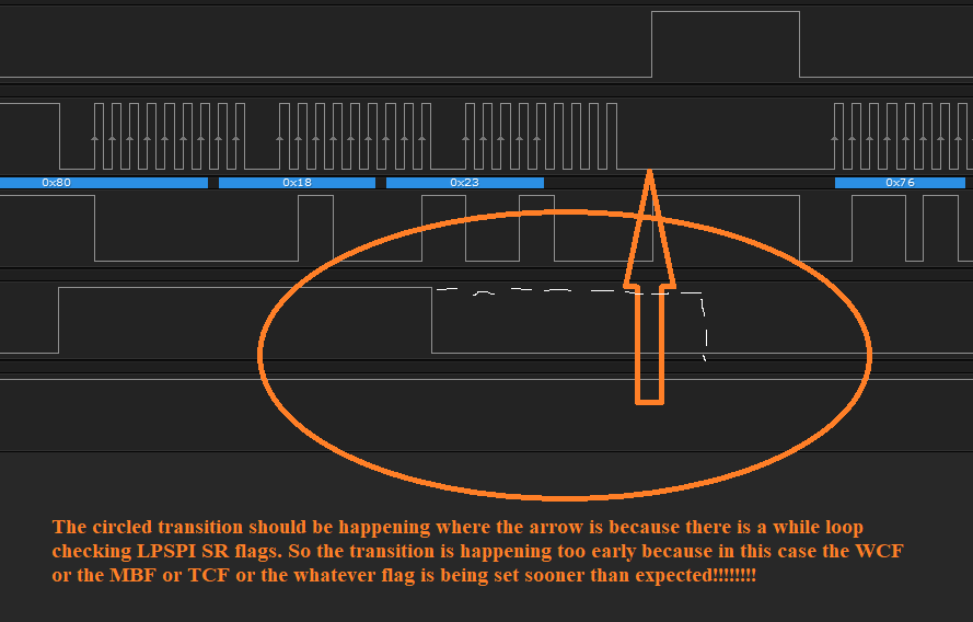
What's the wave line in your red circle? SPI_CS pin? or your LCD gpio pin toggle status?
You want to get the precise point that all the SPI data is shift out to the SPI bus, right?
In fact, the Register is mainly indicate all the data is sent to the SPI buffer, not the real position to the spi bus. I have a suggestion, whether you can use the CS pin, after the SPI tranfer is finished ,and also detect the CS is high, then you can toggle your external GPIO pins.
Wish it helps you!
If you still have questions about it, please kindly let me know!
Best Regards,
Kerry
-------------------------------------------------------------------------------
Note:
- If this post answers your question, please click the "Mark Correct" button. Thank you!
- We are following threads for 7 weeks after the last post, later replies are ignored
Please open a new thread and refer to the closed one, if you have a related question at a later point in time.
-----------------------------------------------------------------------------
- 新着としてマーク
- ブックマーク
- 購読
- ミュート
- RSS フィードを購読する
- ハイライト
- 印刷
- 不適切なコンテンツを報告
Ok,
I am using the mimxrt1060-evk development board. I'm using LPSPI1 with the the following configuration
GPIO_SD_B0_01 -- cs -- GPIO_IO13
GPIO_SD_BO_02 -- mosi
GPIO_SD_BO_03 -- miso
GPIO_SD_BO_00 -- clk
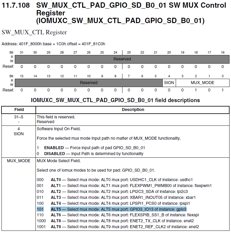
I included my initialization in my previous post and modified the IOMUXC SW_MUX_CTL_PAD_GPIO_SD_B0_01 to have the value of 0x14 -- SION - ON, ALT Func 4.
then added the at the end of my WriteCmdData() function, and not surprisingly it didn't work. It sits in an infinite loop because DR bit 13 is always '0', I tried using the GPIO3->PSR and again IT DOES NOT WORK. So what is missing?
IOMUXC->SW_MUX_CTL_PAD[107] = 0x04 | 0x10; // *GPIO_AD_SD_B0_01 - cs - alt4, output, enable SION
.....
do
{
	tmp = GPIO3->DR; //GPIO->PSR
	__ISB();
	__DSB();
	__asm__("nop");
	__asm__("nop");
	__asm__("nop");
	__asm__("nop");
	tmp &= (1<<13);
}while(!tmp);
- 新着としてマーク
- ブックマーク
- 購読
- ミュート
- RSS フィードを購読する
- ハイライト
- 印刷
- 不適切なコンテンツを報告
Hi rtilson,
Thanks for your updated information.
Just from your wave, the CS pin pull high whould can meet your demand to detect the data is finished.
Then, I think you can also connect CS pin to another GPIO pin to detected it.
You can't just modify GPIO_SD_B0_01 pin as the GPIO, as this is the CS output pin, you need to control it as the SPI_CS pin.
Just from the SPI IP module, it just can indicate that the data is output to the buffer, or the buffer is empty.
It can't dectect the bus directly.
But, another way for you.
You can check your wave, after you send the data out to the SPI_BUF, you can use an timer to check that time, then in your real application, you can add the fixed delay after you send the data to the SPI TX buffer, although that is not precise, but I think it is the useful way in the real application.
You GPIO issues that always in the loop, it is caused that when you change the GPIO_SD_B0_01 to GPIO pin, if you don't configure it, it is the GPIO input pin, and that is not the SPI_CS pin anymore. That way is not good, you may need another GPIO to connect to your real SPI_CS pin.
But I think this way is not good than just add the delay in your SPI tranfer code.
wish it helps you!
Wish it helps you!
If you still have questions about it, please kindly let me know!
Best Regards,
Kerry
-------------------------------------------------------------------------------
Note:
- If this post answers your question, please click the "Mark Correct" button. Thank you!
- We are following threads for 7 weeks after the last post, later replies are ignored
Please open a new thread and refer to the closed one, if you have a related question at a later point in time.
-----------------------------------------------------------------------------
- 新着としてマーク
- ブックマーク
- 購読
- ミュート
- RSS フィードを購読する
- ハイライト
- 印刷
- 不適切なコンテンツを報告
Wasn't the purpose of SION for this type of situation? The peripheral changes the state of the pad and the software is able to read back the state of that pad regardless of that its current function.
Using a delay in an idle loop system is never a good idea. It constrains the speed of the system to the longest of your transmissions.
Can you please provide a description and when I would use the following Status Register flags?
WCF - Word Complete Flag - This is what I use currently to determine when the last bit goes out, but the description has it saying when all input bits has been completely sampled.
FCF - Frame Complete Flag - I would understand to mean that when the last bit goes out and PCS de-asserts
TCF - Transfer Complete Flag - This one I originally thought this flag would be toggled when the last bit goes out on the wire, but CS has not de-asserted
MBF - Module Busy Flag - When is this flag controlled by hardware?
- 新着としてマーク
- ブックマーク
- 購読
- ミュート
- RSS フィードを購読する
- ハイライト
- 印刷
- 不適切なコンテンツを報告
Hi rtilson,
Thanks so much for your updated information.
I also receive your DFAE's case for you about the same question.
Now, talk about my thought and your question and my test result.
1. About the GPIO SION
We may misunderstand the SION function, as today, I also do the SPI_CS pin then set the SION=1, but GPIO data buffer always 0 although the SPI_CS pin is 1 in the bus.
Then I search internally, I find some other similar case, that is mentioned it is not used for other modules, it needs the pin function mux is GPIO, not other module mux
Anyway, I help you double-check with our internal side again. The detail usage of SION.
2. About Status Register flags questions:
All your mentioned Flag is controlled by the SPI hardware module.
WCF - Word Complete Flag - This is what I use currently to determine when the last bit goes out, but the description has it saying when all input bits has been completely sampled.
Answer: My understanding is, as you know, LPSPI have output and input in the same time.
When sendout the data, it also read the input received word.
But in the RM, it mainly mentioned:
Word complete, last bit of word has been sampled.
The Word Complete Flag will set when the last bit of a received word is sampled.
0b - Transfer of a received word has not yet completed
1b - Transfer of a received word has completed
So, this bit is mainly used for the received word sample complete or not.
FCF - Frame Complete Flag - I would understand to mean that when the last bit goes out and PCS de-asserts
Answer: From RM, it mentioned
Frame Complete Flag
The Frame Complete Flag will set at the end of each frame transfer, when the PCS negates.
0b - Frame transfer has not completed
1b - Frame transfer has completed
So, it will indicate the Fram transfer is finished and when the PCS is negates.
TCF - Transfer Complete Flag - This one I originally thought this flag would be toggled when the last bit goes out on the wire, but CS has not de-asserted
Answer: From Rm:
Transfer complete, PCS has negated and transmit/command FIFO is empty.
In master mode when the LPSPI returns to idle state with the transmit FIFO empty, the Transfer
Complete Flag will set.
0b - All transfers have not completed
1b - All transfers have completed
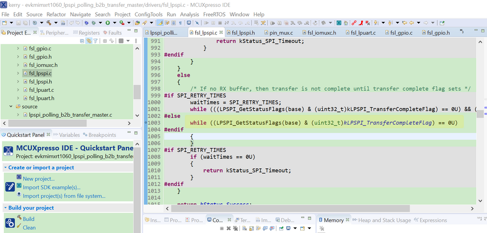
I think this is the useful bit to you to check the status.
I also check the SDK code, in the LPSPI_MasterTransferBlocking API, it also use this bit to check the transmit is finished.
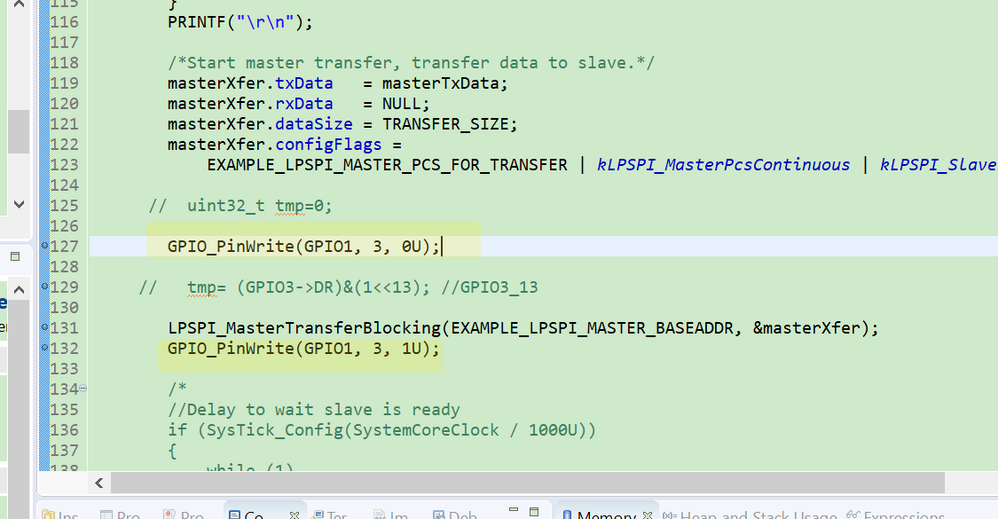
And in fact, I also test the code on my side. I use the GPIO toggle, after the data is sendout, the gpio is pul up after the CS is pull up.
MBF - Module Busy Flag - When is this flag controlled by hardware?
Answer: Module Busy Flag
0b - LPSPI is idle
1b - LPSPI is busy
This bit indicate that the SPI is busy performing a SPI bus transfer.
It is the bus busy flag.
3. My test result.
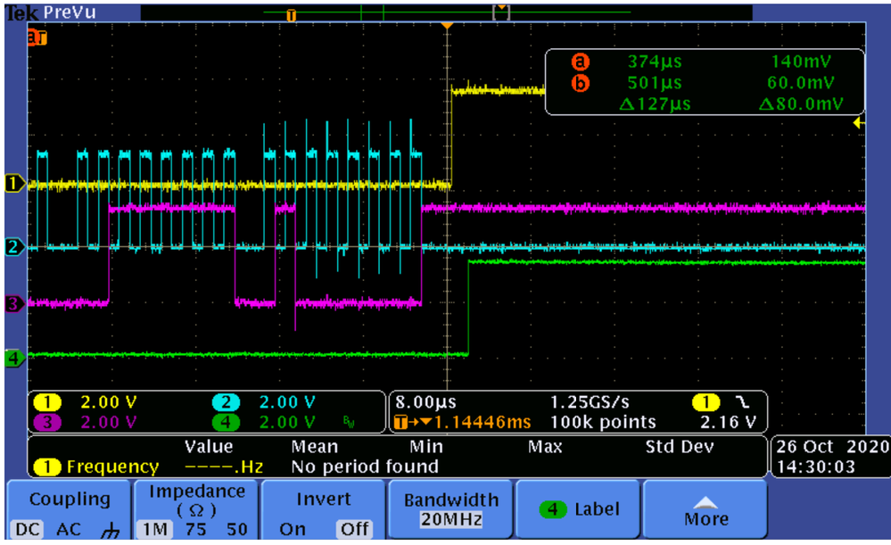
I use the IOMUXC_GPIO_AD_B0_03_GPIO1_IO03 pin as the GPIO pin to indicate the SPI Bus status.
CH1:SPI_CS
CH2:SPI_CLK
CH3:SPI_MOSI
CH4:GPIO1_3
So, you can find, even with the API to sendout, and the GPIO to pull up, you can find the SPI bus already send out all the data.
Please check whether this test result meets your demand?
I also attach my test project with MCUXPresso IDE.
If you still have issues, you also can share me your test project which can reproduce your issues in the MIMXRT1060-EVK board, then I will help you to test it together, and analyzer the issues, and find the solutions.
Best Regards,
Kerry
- 新着としてマーク
- ブックマーク
- 購読
- ミュート
- RSS フィードを購読する
- ハイライト
- 印刷
- 不適切なコンテンツを報告
Thank you for your analysis and time at looking at my issue, I am appreciative of the help. I am interested in hearing about that SION bit because it seems like a big time miss if it can't be used to read the current state of a pad that is not being controlled by the GPIO module.
Before the end of Friday I was successful in getting the desired operation of the peripheral via splitting into 2 separate function calls when I'm trying to get send command and/or send data. If I didn't have to toggle an asynchronous signal in middle of a transaction this wouldn't be a problem.
The function for sending a command uses the TCR[CONT & CONTC] = 0 and I can poll on either FCF or WCF.
The function for sending data used TCR[CONT & CONTC] = 1 (0x3) and I poll on WCF, because my TCR[FRAMESZ] indicates 8 bits.
When I send a command, my TCR[FRAMESZ] = 7 (for 8 bits, this really should be mentioned in the RM, the off by one isn't brought to light) and TCR[CONT/CONTC]=0. I then have to poll on the WCF flag, even though the RM mentioned it for reading data, its the only flag that will toggle on the falling edge of the last clock cycle before CS goes high.
Now, I can poll SR[FCF] if I want and I get a better timing margin when I cycle my asynchronous Data/nCmd signal, because its not a continuous transmission and my command size is 8 bits. This flag toggles when CS is de-asserted as stated in the RM. This is good flag to wait on and arguably better than WCF but both accomplishes what I want.
If I were using the FSR[TXCOUNT] then I can watch the TDF flag when I need to load more data into the FIFO, while keeping in mind that writes to the TCR also occupy TDR FIFO space.
Checking the SR[MBF] from what I've been able to determine with my rudimentary use of this peripheral is to ensure an asynchronous access to the peripheral isn't done while its busy. For my use case its not very useful since all accesses are done on a "continue when done" status check.
My difficulty came from when I wanted to change the TCR[CONT & CONTC] bits to 1 (0x3). The SR[FCF] becomes useless. If you wait on it, then the peripheral will loop until your capture ends and you will capture a continuous stream of 0xFF, which is needed if you need to read data in, while in master mode (no clue in slave mode). I think TCR[FRAMESZ] comes into play when polling on the SR[WCF]. I am operating on an 8bit boundary so SR[WCF] toggles on the last clock cycle every 8bits, if it were 24bits or 32bits then it would be toggling on falling edge of the last clock cycle every 3 to 4 bytes, respectively. I didn't test this but I'm suspecting is the case.
To answer how to control the loop is then to watch your FSR[RXCOUNT] and make sure you are reading it on a regular cycle at the correct TCR[FRAMESZ] width.
One last thing.
Peripheral clocking. The clock that controls the peripheral. I have the peripheral running on PLL2/6 (528MHz/6 = 88MHz) I found that my explanation above fails apart when its running at div-5 or lower. I am not using the TCR[PRESCALE] = 0x0 and I have CCR[SCKPCS], CCR[PCSSCK], set to max delay and CCR[DBT] = 0x7F and CCR[SCKDIV] = 0x50.
For my application, these parameters work and get good enough throughput at a TCR[FRAMESZ] = 7(8 bits). It can be improved if the frame size is adjust accordingly.
If I had to RCA this. Clocking requirements of the peripheral aren't clearly stated and I don't think I have a complete understanding on how fast I can run it but, for what I'm doing this is fine. A simple explanation of how the Flags are used in a given situation would help with simple code to compliment the explanation would be nice. I found that the SDK code looks extremely complex and completely obfuscates what the hardware is doing. At least that is my opinion. Polling with this peripheral is a challenge and is better suited for asynchronous use through either EDMA or Interrupt Handling.
I hope this makes sense and is an adequate explanation of what I have learned.
- 新着としてマーク
- ブックマーク
- 購読
- ミュート
- RSS フィードを購読する
- ハイライト
- 印刷
- 不適切なコンテンツを報告
I am incorrect about the Framesz being off by one. It is stated in Table 48-3. My apologies.
- 新着としてマーク
- ブックマーク
- 購読
- ミュート
- RSS フィードを購読する
- ハイライト
- 印刷
- 不適切なコンテンツを報告
Hi rtilson,
Thanks so much for your detail updated information, and sorry for the later reply because these days a lot of cases in the queue, thanks a lot for your understanding.
Now, talk back about your issues again:
1. About the GPIO SION
I have checked with our internal expert, the SION just can be used when the MUX is the GPIO, then customer can use the PSR to check the pin status.
When configure the MUX as SPI_CS, then even SION is set, we can't use the GPIO PSR to detect the pin situation, the expert already confirm it, and you and my test result also confirm it. So, the SION function with SPI_CS may not useful to you.
2. About the peripheral clocking
Please check the RT1060 datasheet, you can find some information about it:
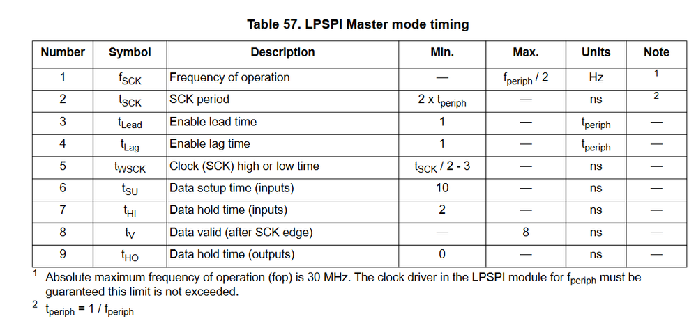
Absolute maximum frequency of operation (fop) is 30 MHz. The clock driver in the LPSPI module for fperiph must be guaranteed this limit is not exceeded.
3. TCR[CONT & CONTC] bits to 1 (0x3)
Do you mean when you use TCR[FRAMESZ] = 7(8 bits), this also gets good enough throughput?
About how the Flags are used in a given situation, I also need to check the internal side, please give me more time.
Please keep the patient, thanks.
Any updated information from my side, I will let you know.
Best Regards,
Kerry
- 新着としてマーク
- ブックマーク
- 購読
- ミュート
- RSS フィードを購読する
- ハイライト
- 印刷
- 不適切なコンテンツを報告
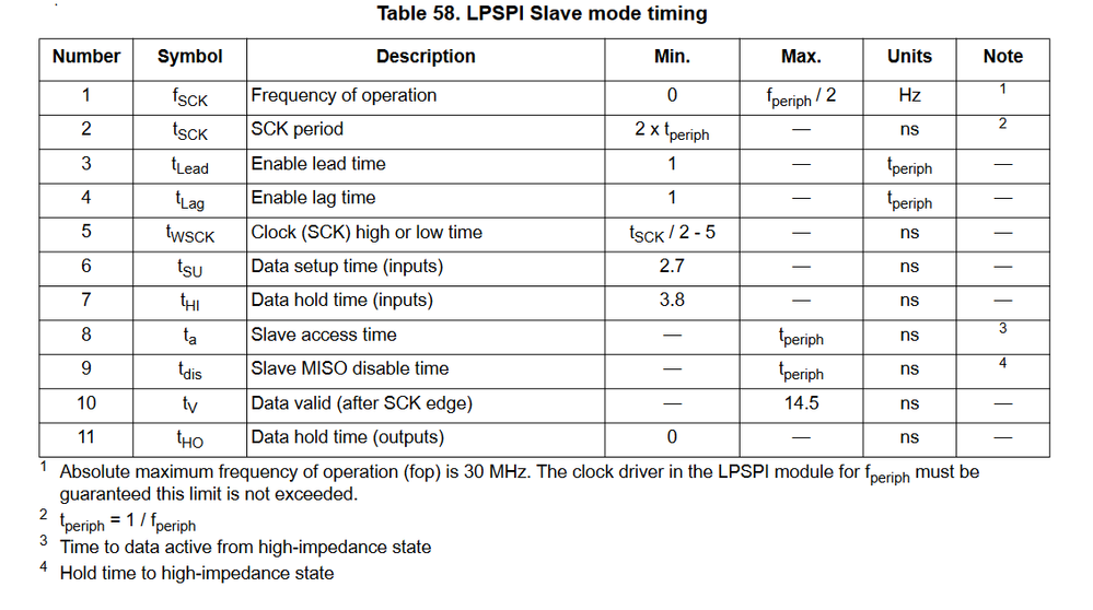
The maximum speed that this peripheral device can be driven at is 30MHz? Could I place a request for that little tidbit be added to the reference manual in the LPSPI section?
I found the 30MHz specification in the datasheet you mentioned but its easily missed.
- 新着としてマーク
- ブックマーク
- 購読
- ミュート
- RSS フィードを購読する
- ハイライト
- 印刷
- 不適切なコンテンツを報告
Hi rtilson,
Yes, what I mentioned is your post picture's note, it mentioned 30Mhz as the max operation frequency.
You can consider the max operation frequency as the sck bit rate, when you set the peripheral frequency, make sure your bit rate smaller than 30Mhz.
You mentioned that the transmission mostly figured out, do you mean when TCR[CONT & CONTC] bits to 1 (0x3), and you detect the detail CS pull high point in the bus now?
Best Regards,
Kerry
- 新着としてマーク
- ブックマーク
- 購読
- ミュート
- RSS フィードを購読する
- ハイライト
- 印刷
- 不適切なコンテンツを報告
You mentioned that the transmission mostly figured out, do you mean when TCR[CONT & CONTC] bits to 1 (0x3), and you detect the detail CS pull high point in the bus now?I still have to loop on the SR[WCF] when using TCR[CONT/CONTC]. The reason being is that SR[TDF] only flags when the TX FIFO is under the water or equal to the water mark. SR[TCF] flags when the peripheral is idle and the FIFO is empty, not very useful when there is is only ever one in the fifo to begin with, in my case and the peripheral never idle when TCR[CONT/CONTC] are set. SR[FCF] flags when the frame is complete. A complete frame in this case is when CS is de-asserted by a write clearing TCR[CONT] and so in my case isn't useful. That leaves SR[WCF], I call this old faithful because it flags on the last clock cycle of the frame reliably, even if TCR[RXMASK] = 1.
I am certain the way I'm using the peripheral is sub-optimal based on its design but I'm just starting out using the RT106x family.
- 新着としてマーク
- ブックマーク
- 購読
- ミュート
- RSS フィードを購読する
- ハイライト
- 印刷
- 不適切なコンテンツを報告
Hi rtilson,
Thanks so much for your updated information.
Now, polling WCF can solve your transfer application usage, but now, your main issue is the receive MISO issues, right? You don't know use which flag to receive the data from the slave or it is not very correct right?
This is the polled rx related testing code:
uint32 lpspi_polled_rx(LPSPI_MemMapPtr module)
{
uint32 data = 0;
/*Wait for RX to be ready
* The receive data flag is set whenever the number of words in the receive
* FIFO is greater than RXWATER
*/
while(!(get_lpspi_sr(module) & get_lpspi_sr_rdf_mask()));
data = get_lpspi_rdr(module);
return data;
}
uint32 get_lpspi_sr_rdf_mask()
{
return (LPSPI_SR_RDF_MASK);
}
uint32 get_lpspi_sr(LPSPI_MemMapPtr module)
{
return (LPSPI_SR_REG(module));
}
uint32 get_lpspi_rdr(LPSPI_MemMapPtr module)
{
return (LPSPI_RDR_REG(module));
}
Best Regards,
Kerry
- 新着としてマーク
- ブックマーク
- 購読
- ミュート
- RSS フィードを購読する
- ハイライト
- 印刷
- 不適切なコンテンツを報告
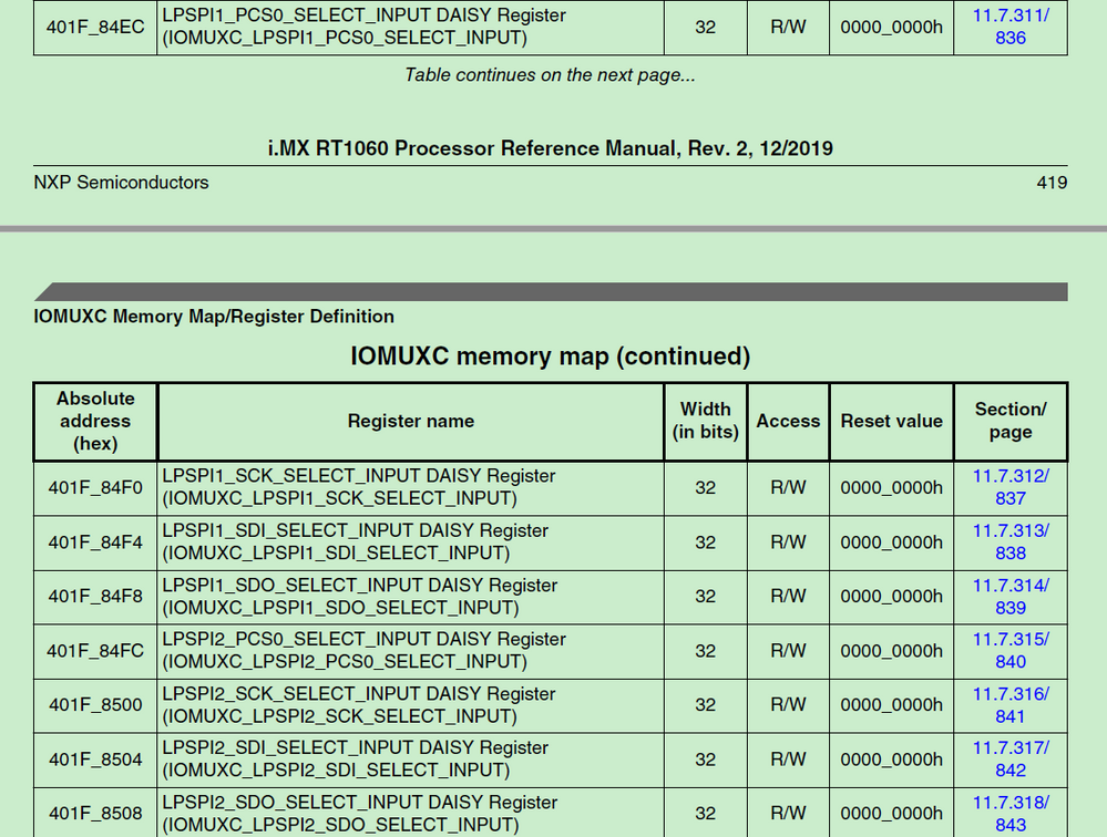
@kerryzhouI solved my problem with MISO enabling Daisy Chaining. I created thread How-do-I-recieve-data-on-the-LPSPI-Bus , and I loaded the simple loopback sdk demo and looked at the the register status while it was running the development board. Apparently, LPSPI1 MISO input controlled via a secondary IOMUXC that selects what signal the actual pad is connected too.
- 新着としてマーク
- ブックマーク
- 購読
- ミュート
- RSS フィードを購読する
- ハイライト
- 印刷
- 不適切なコンテンツを報告
Hi rtilson,
Daisy Chaining is used to configure the pin function, so your previous issue is still in the pin function configuration.
In fact, a lot of pins have the DAISY register, you can check the RM:
It is determined by which detail pin you have selected.
Take an example, if your pin is just the DAISY=0 which is the default one, then even you don't enable the DAISY, you also don't have issues. But if your select pin is DAISY=1, then you need to configure the DAISY.
Thanks for your root issue sharing.
If you still have issues, just kindly let us know.
Wish it helps you!
If you still have questions about it, please kindly let me know!
Best Regards,
Kerry
-------------------------------------------------------------------------------
Note:
- If this post answers your question, please click the "Mark Correct" button. Thank you!
- We are following threads for 7 weeks after the last post, later replies are ignored
Please open a new thread and refer to the closed one, if you have a related question at a later point in time.
-----------------------------------------------------------------------------
- 新着としてマーク
- ブックマーク
- 購読
- ミュート
- RSS フィードを購読する
- ハイライト
- 印刷
- 不適切なコンテンツを報告
The reference manual section for LPSPI doesn't mention that the pin could possibly be shared and have to be daisy chained. You sort of have to know that is something you have to check when configuring the peripheral pins. The reset value of that daisy chain defaults to a different pin and that is something that I missed and didn't think to check.

