- Forums
- Product Forums
- General Purpose MicrocontrollersGeneral Purpose Microcontrollers
- i.MX Forumsi.MX Forums
- QorIQ Processing PlatformsQorIQ Processing Platforms
- Identification and SecurityIdentification and Security
- Power ManagementPower Management
- MCX Microcontrollers
- S32G
- S32K
- S32V
- MPC5xxx
- Other NXP Products
- Wireless Connectivity
- S12 / MagniV Microcontrollers
- Powertrain and Electrification Analog Drivers
- Sensors
- Vybrid Processors
- Digital Signal Controllers
- 8-bit Microcontrollers
- ColdFire/68K Microcontrollers and Processors
- PowerQUICC Processors
- OSBDM and TBDML
-
- Solution Forums
- Software Forums
- MCUXpresso Software and ToolsMCUXpresso Software and Tools
- CodeWarriorCodeWarrior
- MQX Software SolutionsMQX Software Solutions
- Model-Based Design Toolbox (MBDT)Model-Based Design Toolbox (MBDT)
- FreeMASTER
- eIQ Machine Learning Software
- Embedded Software and Tools Clinic
- S32 SDK
- S32 Design Studio
- GUI Guider
- Zephyr Project
- Voice Technology
- Application Software Packs
- Secure Provisioning SDK (SPSDK)
- Processor Expert Software
- MCUXpresso Training Hub
-
- Topics
- Mobile Robotics - Drones and RoversMobile Robotics - Drones and Rovers
- NXP Training ContentNXP Training Content
- University ProgramsUniversity Programs
- Rapid IoT
- NXP Designs
- SafeAssure-Community
- OSS Security & Maintenance
- Using Our Community
-
- Cloud Lab Forums
-
- Knowledge Bases
JTAG_MOD settings for i.MX 8M Nano
According to the reference manual of the i.MX 8M Mini, in order to enable the IEEE1149.1 standard features of the JTAG interface, the TEST_MODE, BOOT_MODE1, BOOT_MODE0, and JTAG_MOD have to be set to 1110. I now saw the exact same note in the reference manual for the i.MX 8M Nano (Rev. 0 12/2019) on page 206. However, this does not make any sense. The i.MX 8M Nano does not have a TEST_MODE pin. On the other hand, the Nano features additionally BOOT_MODE2 and BOOT_MODE3.
How do the pins need to be strapped on the i.MX 8M Nano for enabling the IEEE1149.1 feature?
Hi @weidong_sun,
I have the same issue as the bill_tucker. When i pulling the BOOT_MODE3_0 signals to "1111" to enter in boundary scan, the LDO2 (VDD_SNVS_0V8) goes to 0.95V. In normal condition when then BOOT_MODE3_0 is "0010" (boot from emmc) the LDO2 is 0.8V.
Measuring the VDD_SNVS_0V8 when the BOOT_MODE3_0 signals are at "1111", a frequency of ~32kHz over the 0.8V level is noted. On our board, the VDD_SNVS_0V8 signal is connected to the RTC_XTALO, according to item 3.1.4 - IMX8MNIEC.pdf.
Could this issue be generated with the connection of VDD_SNVS_0V8 with RTC_XTALO?
Is there any solution to this issue?
Regards,
Estiven
Hi Peter,
JTAG_MOD is not related to BOOT_MODE pins.
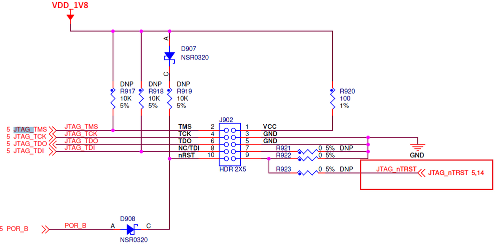
Below is that of I.MX8MM EVK and i.MX8MN
Handling method of 2 boards is to pull JTAG_MOD pin to LOW.
Here is BOOT_MODE of 2 boards:
Both SOM boards use the same Base board:
I.MX8M Mini : BOOT_MODE0 & BOOT_MODE1,JTAG_nTRST & TEST_MODE pins.
i.MX8M Nano: BOOT_MODE0/BOOT_MODE1/BOOT_MODE2/BOOT_MODE3, no TEST_MODE & JTAG_nTRST.
[comment]
--TEST_MODE pin: the pin is for CPU's test mode or normal working mode. when CPU works normally, the pin should be pulled down to LOW.
--JTAG_nTRST pin: For JTAG port, the signal is optional. about this, ARM has a detailed description.
See the link, please!
ARM Information Center
Then you can find JTAG interface on base board of these 2 boards:
Hope above information is helpful for you!
Have a nice day!
B.R,
Weidong
Hi weidong.sun
Thank you for the fast reply. Are you sure that the strapping of the TEST_MODE, BOOT_MODE1, and BOOT_MODE0 are irrelevant for going into the IEEE1149.1 compliant JTAG mode on the i.MX 8M Mini? We have our own i.MX 8M Mini based computer module. The TEST_MODE, BOOT_MODE1, and BOOT_MODE0 are all set to 0 since this is what we need for the final product to boot correctly. However, in production testing, we need to be able to use boundary-scan. As with other i.MX based products, we just set the JTAG_MOD to 0 for going into this mode. Unfortunately, we faced an issue as the read back JTAG ID is wrong. In order to fix that, we need to set the TEST_MODE, BOOT_MODE1, and BOOT_MODE0 to 1. This is quite ugly since we need now a circuit that allows us to change the level of the TEST_MODE, BOOT_MODE1, and BOOT_MODE0 only during production testing.
I was creating this ticket since I was wondering whether the same issue exists also for the i.MX 8M Nano. I need to know whether we need to add also a circuit on these products in order to use the boundary scan mode during production testing.
All
I can get the boundary scan mode to work on the Nano by pulling BOOT_MODE3_0 to "1111" via 4.7k resistors and JTAG_Mod to "0"
However, the LDO2 of the BD71847 (VDD_SNVS_0V8) goes to 0.95V from 0.8V when this is done.
Anybody else observe that?
If I don't pull BOOT_MODE3_0 to all 1s, the LDO2 voltage is normal.
Bill Tucker
Hi @weidong_sun,
I have the same issue as the bill_tucker. When i pulling the BOOT_MODE3_0 signals to "1111" to enter in boundary scan, the LDO2 (VDD_SNVS_0V8) goes to 0.95V. In normal condition when then BOOT_MODE3_0 is "0010" (boot from emmc) the LDO2 is 0.8V.
Measuring the VDD_SNVS_0V8 when the BOOT_MODE3_0 signals are at "1111", a frequency of ~32kHz over the 0.8V level is noted. On our board, the VDD_SNVS_0V8 signal is connected to the RTC_XTALO, according to item 3.1.4 - IMX8MNIEC.pdf.
Could this issue be generated with the connection of VDD_SNVS_0V8 with RTC_XTALO?
Is there any solution to this issue?
Regards,
Estiven
Hello Pert,
i.MX Expert gave us feedback, I will send it to you by personal email.
check your email, please!
Weidong
OK, Peter, I will submit your question to i.mx expert team.
Ask for expert's help.
Wait for my feedback, please!
Have a nice day!
B.R
Weidong


