- Forums
- Product Forums
- General Purpose MicrocontrollersGeneral Purpose Microcontrollers
- i.MX Forumsi.MX Forums
- QorIQ Processing PlatformsQorIQ Processing Platforms
- Identification and SecurityIdentification and Security
- Power ManagementPower Management
- MCX Microcontrollers
- S32G
- S32K
- S32V
- MPC5xxx
- Other NXP Products
- Wireless Connectivity
- S12 / MagniV Microcontrollers
- Powertrain and Electrification Analog Drivers
- Sensors
- Vybrid Processors
- Digital Signal Controllers
- 8-bit Microcontrollers
- ColdFire/68K Microcontrollers and Processors
- PowerQUICC Processors
- OSBDM and TBDML
- S32M
-
- Solution Forums
- Software Forums
- MCUXpresso Software and ToolsMCUXpresso Software and Tools
- CodeWarriorCodeWarrior
- MQX Software SolutionsMQX Software Solutions
- Model-Based Design Toolbox (MBDT)Model-Based Design Toolbox (MBDT)
- FreeMASTER
- eIQ Machine Learning Software
- Embedded Software and Tools Clinic
- S32 SDK
- S32 Design Studio
- GUI Guider
- Zephyr Project
- Voice Technology
- Application Software Packs
- Secure Provisioning SDK (SPSDK)
- Processor Expert Software
- MCUXpresso Training Hub
-
- Topics
- Mobile Robotics - Drones and RoversMobile Robotics - Drones and Rovers
- NXP Training ContentNXP Training Content
- University ProgramsUniversity Programs
- Rapid IoT
- NXP Designs
- SafeAssure-Community
- OSS Security & Maintenance
- Using Our Community
-
- Cloud Lab Forums
-
- Knowledge Bases
- ARM Microcontrollers
- i.MX Processors
- Identification and Security
- Model-Based Design Toolbox (MBDT)
- QorIQ Processing Platforms
- S32 Automotive Processing Platform
- Wireless Connectivity
- CodeWarrior
- MCUXpresso Suite of Software and Tools
- MQX Software Solutions
-
- Home
- :
- i.MX Forums
- :
- i.MX Processors
- :
- Re: About Input the Osc clock (32.768kHz) during i.MX6 power off.
About Input the Osc clock (32.768kHz) during i.MX6 power off.
- Subscribe to RSS Feed
- Mark Topic as New
- Mark Topic as Read
- Float this Topic for Current User
- Bookmark
- Subscribe
- Mute
- Printer Friendly Page
- Mark as New
- Bookmark
- Subscribe
- Mute
- Subscribe to RSS Feed
- Permalink
- Report Inappropriate Content
Dear All,
Hello. My customer has used i.MX 6Dual and PF0100.
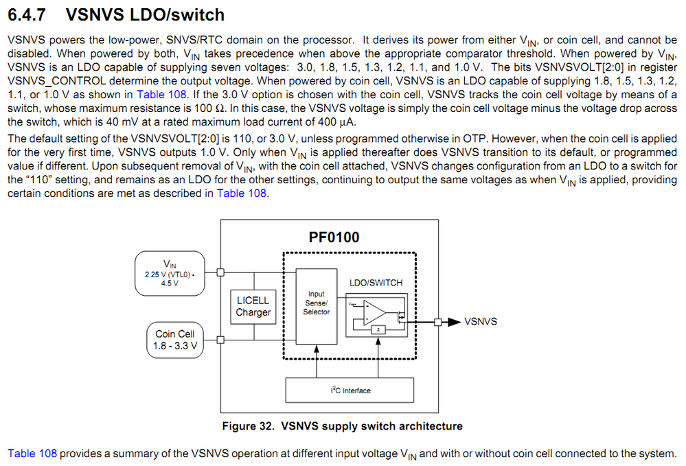
PF0100's VSNVS output starts from 1.0 V when LICELL is valid before VIN.
*Refer to "Figure 6. Default start-up sequence" in MMPF0100Z(Rev.10).
And, the VSNVS output to external oscillator (32.768kHz), too.
But, the oscillator started the operation at 1V.
The Osc clock has been inputted to i.MX6 with power off.
(VDD_SNVS_CAP was 0V. So internal LDO looks disabled.)
*Refer to attached system structure.
[Question]
Does the Osc clock give i.MX damage during above situation?
(Or, is there possibility to destroy the i.MX6 device?)
Amplitude of osc clock was measured 1.1V.
Best Regards,
Keita
Solved! Go to Solution.
- Mark as New
- Bookmark
- Subscribe
- Mute
- Subscribe to RSS Feed
- Permalink
- Report Inappropriate Content
It does not help since the RTC_XTALI input is still out of spec all the time. The Table 21 of the i.MX6Dual/Quad Data Sheet document clearly says that the maximum allowed RTC_XTALI input voltage is no higher than 1.1V. Anyway, to guarantee the long-term stability and reliability of their system, your customer has to redesign their RTC_XTALI clock source.
Artur
- Mark as New
- Bookmark
- Subscribe
- Mute
- Subscribe to RSS Feed
- Permalink
- Report Inappropriate Content
1. It _is_the_problem_ since the RTC_XTALI is _higher_ than VDD_SNSV_CAP in all case you've shown.
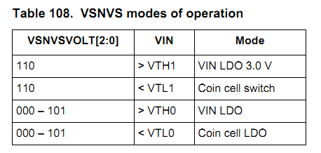
2. The MMPF0100 Data Sheet Rev.15 document says the following.
So, ask the customer to check the VSNVS settings.
Artur
- Mark as New
- Bookmark
- Subscribe
- Mute
- Subscribe to RSS Feed
- Permalink
- Report Inappropriate Content
Dear Artur,
Hello. Thank you for your reply.
> 1. It _is_the_problem_ since the RTC_XTALI is _higher_ than VDD_SNSV_CAP in all case you've shown.
You are right. Sorry for my misunderstanding.
For example, refer to "Figure 6. Default start-up sequence" in MMPF0100Z Rev.10.
If it is right sequence, VSNVS keeps the 1V output during 3.0 [msec].
tR1 : Rise time of VSNVS : Typ 3.0 ms
In this case, I think that it is no problem because of the very short period(3ms).
Is my understanding OK?
> 2. The MMPF0100 Data Sheet Rev.15 document says the following.
This issue happened before I2C communication.
So, user can't set this register.
My customer is using "NP" device with TBB mode now.
So, the VSNVS output 1V until starting the I2C communication.
Best Regards,
Keita
- Mark as New
- Bookmark
- Subscribe
- Mute
- Subscribe to RSS Feed
- Permalink
- Report Inappropriate Content
Anyway, according to the oscilloscope screenshots your customer has provided, RTC_XTALI is always higher than VDD_SNVS_CAP, so, it is still the problem.
Artur
- Mark as New
- Bookmark
- Subscribe
- Mute
- Subscribe to RSS Feed
- Permalink
- Report Inappropriate Content
Dear Artur,
Hello.
>Anyway, according to the oscilloscope screenshots your customer has provided, D is always higher than >VDD_SNVS_CAP, so, it is still the problem.
Yes. You are right. But, my customer can't do a big change on their schematic because MP schedule is critical.
So, my customer will change the PWRON timing early.
If the input timing is same VIN and PWRON, the above 3 msec limitation will be occurred.
Please confirm the below question.
========
For example, refer to "Figure 6. Default start-up sequence" in MMPF0100Z Rev.10.
In right sequence, VSNVS keeps the 1V output during 3.0 [msec].
tR1 : Rise time of VSNVS : Typ 3.0 ms
In this case, I think that it is no problem because of the very short period(only 3ms) with "RTC_XTALI > VDD_SNVS_CAP".
Is my understanding OK?
========
When it isn't possible to be permissible by this 3msec limitation, i.MX6 can not be used in the SNVS mode...
The SNVS output (=1V) is spec-out from VDD_SNVS_IN spec. in i.MX6
Best Regards,
Keita
- Mark as New
- Bookmark
- Subscribe
- Mute
- Subscribe to RSS Feed
- Permalink
- Report Inappropriate Content
It does not help since the RTC_XTALI input is still out of spec all the time. The Table 21 of the i.MX6Dual/Quad Data Sheet document clearly says that the maximum allowed RTC_XTALI input voltage is no higher than 1.1V. Anyway, to guarantee the long-term stability and reliability of their system, your customer has to redesign their RTC_XTALI clock source.
Artur
- Mark as New
- Bookmark
- Subscribe
- Mute
- Subscribe to RSS Feed
- Permalink
- Report Inappropriate Content
Dear Keita,
In any case, the amplitude of an external RTC_XTALI clock signal must not exceed VDD_SNVS_CAP, that is typically around 1.0V in working conditions. Otherwise, a permanent chip damage may occur. As far as I can see on the oscilloscope screenshots you've provided, this requirement is not met in your customer's system. In the current state, the system is non-functional since it does not meet the RTC_XTALI input specs. The level of an external clock signal must be aligned to VDD_SNVS_CAP. For that, some level shifting circuit must be used.
Another point is that they use wrong LICELL voltage to backup the system. For normal operation, the LICELL voltage must be at around 3.0V - 3.3V level.
Have a great day,
Artur
-----------------------------------------------------------------------------------------------------------------------
Note: If this post answers your question, please click the Correct Answer button. Thank you!
-----------------------------------------------------------------------------------------------------------------------
- Mark as New
- Bookmark
- Subscribe
- Mute
- Subscribe to RSS Feed
- Permalink
- Report Inappropriate Content
Dear Artur,
Hello. Thank you for your reply.
[Q1]
>In any case, the amplitude of an external RTC_XTALI clock signal must not exceed VDD_SNVS_CAP,
>that is typically around 1.0V in working conditions.
- Amplitude of an external RTC_XTALI clock signal = 1.1V
- VDD_SNVS_CAP = 0.4V
So, I think that it is no problem because RTC_XTALI clock signal was not exceed than VDD_SNVS_CAP?
Is my understanding OK?
[Q2]
> Another point is that they use wrong LICELL voltage to backup the system.
> For normal operation, the LICELL voltage must be at around 3.0V - 3.3V level.
Why are you think that my customer uses wrong LICELL voltage??
I think that my customer uses LICELL voltage at 3V.
The below comment is PF0100's function.
PF0100's VSNVS output starts from 1.0 V when LICELL is valid before VIN.
Best Regards,
Keita
- Mark as New
- Bookmark
- Subscribe
- Mute
- Subscribe to RSS Feed
- Permalink
- Report Inappropriate Content
To make me able to check the issue, please provide the ramp-up curves of both VDD_SNVS_IN and VDD_SNVS_CAP voltages with relation to the oscillator output curves once the battery is applied.
Best Regards,
Artur
- Mark as New
- Bookmark
- Subscribe
- Mute
- Subscribe to RSS Feed
- Permalink
- Report Inappropriate Content
Dear Artur,
Hello. I got the waveform. Please check the attached file.
Sorry. I misunderstood about below comment.
===
VDD_SNVS_CAP was 0V.
So internal LDO looks disabled.
===
The correct information was below.
===
VDD_SNVS_IN was 1.0V.
VDD_SNVS_CAP was 0.4V.
So internal LDO looks enabled.
===
Best Regards,
Keita
- Mark as New
- Bookmark
- Subscribe
- Mute
- Subscribe to RSS Feed
- Permalink
- Report Inappropriate Content
Dear Artur,
Thank you for your reply.
OK. I requested my customer to get the waveform.
VDD_SNVS_CAP was 0V.
So internal LDO looks disabled.
And, the customer's product has the possibility that the following condition continues.
"PF0100's VSNVS output starts from 1.0 V when LICELL is valid before VIN."
Best Regards,
Keita
- Mark as New
- Bookmark
- Subscribe
- Mute
- Subscribe to RSS Feed
- Permalink
- Report Inappropriate Content
Hi All,
Do you have any update?
Our customer is urging us to answer the item quickly.
Best Regards,
Keita

