- NXP Forums
- Product Forums
- General Purpose MicrocontrollersGeneral Purpose Microcontrollers
- i.MX Forumsi.MX Forums
- QorIQ Processing PlatformsQorIQ Processing Platforms
- Identification and SecurityIdentification and Security
- Power ManagementPower Management
- MCX Microcontrollers
- S32G
- S32K
- S32V
- MPC5xxx
- Other NXP Products
- Wireless Connectivity
- S12 / MagniV Microcontrollers
- Powertrain and Electrification Analog Drivers
- Sensors
- Vybrid Processors
- Digital Signal Controllers
- 8-bit Microcontrollers
- ColdFire/68K Microcontrollers and Processors
- PowerQUICC Processors
- OSBDM and TBDML
-
- Solution Forums
- Software Forums
- MCUXpresso Software and ToolsMCUXpresso Software and Tools
- CodeWarriorCodeWarrior
- MQX Software SolutionsMQX Software Solutions
- Model-Based Design Toolbox (MBDT)Model-Based Design Toolbox (MBDT)
- FreeMASTER
- eIQ Machine Learning Software
- Embedded Software and Tools Clinic
- S32 SDK
- S32 Design Studio
- GUI Guider
- Zephyr Project
- Voice Technology
- Application Software Packs
- Secure Provisioning SDK (SPSDK)
- Processor Expert Software
- MCUXpresso Training Hub
-
- Topics
- Mobile Robotics - Drones and RoversMobile Robotics - Drones and Rovers
- NXP Training ContentNXP Training Content
- University ProgramsUniversity Programs
- Rapid IoT
- NXP Designs
- SafeAssure-Community
- OSS Security & Maintenance
- Using Our Community
-
- Cloud Lab Forums
-
- RSS フィードを購読する
- トピックを新着としてマーク
- トピックを既読としてマーク
- このトピックを現在のユーザーにフロートします
- ブックマーク
- 購読
- ミュート
- 印刷用ページ
- 新着としてマーク
- ブックマーク
- 購読
- ミュート
- RSS フィードを購読する
- ハイライト
- 印刷
- 不適切なコンテンツを報告
Hi
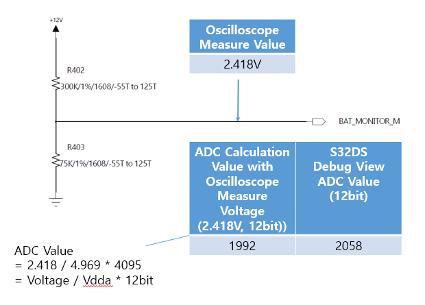
I compared actual voltage to ADC value.
but, those value were quite different.
I proceeded as follows.
could you tell me why calculating value is different with ADC value?
and do I have to what to check?
Regards,
Jongchan.
解決済! 解決策の投稿を見る。
- 新着としてマーク
- ブックマーク
- 購読
- ミュート
- RSS フィードを購読する
- ハイライト
- 印刷
- 不適切なコンテンツを報告
Hi Jongchan,
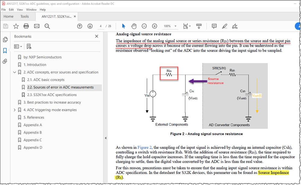
Please refer: AN12217, S32K1xx ADC guidelines, spec and configuration
The impedance of the analog signal source or series resistance (RIN) between the source and the input pin causes a voltage drop across it because of the current flowing into the pin. It can be understood as the resistance observed “looking out” of the ADC into the source driving the input signal to be sampled.
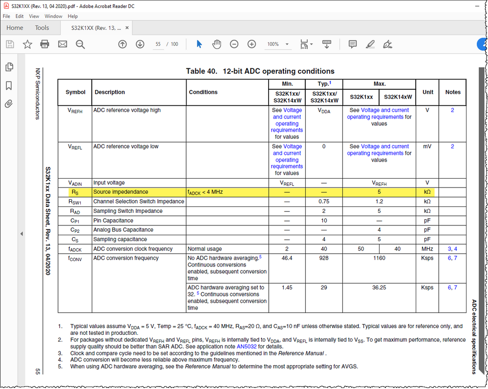
For this reason, precautions must be taken to ensure that the analog input signal source resistance is within ADC specification. In the datasheet for S32K devices, this parameter can be found as Source Impedance (RS).
Best Regards,
Robin
-------------------------------------------------------------------------------
Note:
- If this post answers your question, please click the "Mark Correct" button. Thank you!
- We are following threads for 7 weeks after the last post, later replies are ignored
Please open a new thread and refer to the closed one, if you have a related question at a later point in time.
-------------------------------------------------------------------------------
- 新着としてマーク
- ブックマーク
- 購読
- ミュート
- RSS フィードを購読する
- ハイライト
- 印刷
- 不適切なコンテンツを報告
Can I understand it this way? If I use an adc clock that is less than 4M, the maximum allowable rs for external circuits is 5k.
If I use an adc clock of 40M, what should be the rs? Why is it not stated in the manual, should it be larger or smaller than 5k?
Thank you.
- 新着としてマーク
- ブックマーク
- 購読
- ミュート
- RSS フィードを購読する
- ハイライト
- 印刷
- 不適切なコンテンツを報告
Hi Jongchan,
Please refer: AN12217, S32K1xx ADC guidelines, spec and configuration
The impedance of the analog signal source or series resistance (RIN) between the source and the input pin causes a voltage drop across it because of the current flowing into the pin. It can be understood as the resistance observed “looking out” of the ADC into the source driving the input signal to be sampled.
For this reason, precautions must be taken to ensure that the analog input signal source resistance is within ADC specification. In the datasheet for S32K devices, this parameter can be found as Source Impedance (RS).
Best Regards,
Robin
-------------------------------------------------------------------------------
Note:
- If this post answers your question, please click the "Mark Correct" button. Thank you!
- We are following threads for 7 weeks after the last post, later replies are ignored
Please open a new thread and refer to the closed one, if you have a related question at a later point in time.
-------------------------------------------------------------------------------


