
- Forums
- Product Forums
- General Purpose MicrocontrollersGeneral Purpose Microcontrollers
- i.MX Forumsi.MX Forums
- QorIQ Processing PlatformsQorIQ Processing Platforms
- Identification and SecurityIdentification and Security
- Power ManagementPower Management
- Wireless ConnectivityWireless Connectivity
- RFID / NFCRFID / NFC
- Advanced AnalogAdvanced Analog
- Neural Processing UnitsNeural Processing Units
- MCX Microcontrollers
- S32G
- S32K
- S32V
- MPC5xxx
- Other NXP Products
- S12 / MagniV Microcontrollers
- Powertrain and Electrification Analog Drivers
- Sensors
- Vybrid Processors
- Digital Signal Controllers
- 8-bit Microcontrollers
- ColdFire/68K Microcontrollers and Processors
- PowerQUICC Processors
- OSBDM and TBDML
- S32M
- S32Z/E
-
- Solution Forums
- Software Forums
- MCUXpresso Software and ToolsMCUXpresso Software and Tools
- CodeWarriorCodeWarrior
- MQX Software SolutionsMQX Software Solutions
- Model-Based Design Toolbox (MBDT)Model-Based Design Toolbox (MBDT)
- FreeMASTER
- eIQ Machine Learning Software
- Embedded Software and Tools Clinic
- S32 SDK
- S32 Design Studio
- GUI Guider
- Zephyr Project
- Voice Technology
- Application Software Packs
- Secure Provisioning SDK (SPSDK)
- Processor Expert Software
- Generative AI & LLMs
-
- Topics
- Mobile Robotics - Drones and RoversMobile Robotics - Drones and Rovers
- NXP Training ContentNXP Training Content
- University ProgramsUniversity Programs
- Rapid IoT
- NXP Designs
- SafeAssure-Community
- OSS Security & Maintenance
- Using Our Community
-
- Cloud Lab Forums
-
- Knowledge Bases
- ARM Microcontrollers
- i.MX Processors
- Identification and Security
- Model-Based Design Toolbox (MBDT)
- QorIQ Processing Platforms
- S32 Automotive Processing Platform
- Wireless Connectivity
- CodeWarrior
- MCUXpresso Suite of Software and Tools
- MQX Software Solutions
- RFID / NFC
- Advanced Analog
- Neural Processing Units
-
- NXP Tech Blogs
- Home
- :
- Product Forums
- :
- S32K
- :
- S32K148: Flash Erase Block Problem
S32K148: Flash Erase Block Problem
- Subscribe to RSS Feed
- Mark Topic as New
- Mark Topic as Read
- Float this Topic for Current User
- Bookmark
- Subscribe
- Mute
- Printer Friendly Page
- Mark as New
- Bookmark
- Subscribe
- Mute
- Subscribe to RSS Feed
- Permalink
- Report Inappropriate Content
Hello,
I am experimenting with the S32K148 internal flash and ran into problems.
What I want to achieve is the following:
Partition the flash area which can be used to emulate EEProm such that it is available as 512K D-Flash partition (compare page 773 in chip's reference manual). After partitioning I want to write a little data at the beginning of this flash partition. From the memory map document attached to the reference manual this partition starts at address 0x1000_0000.
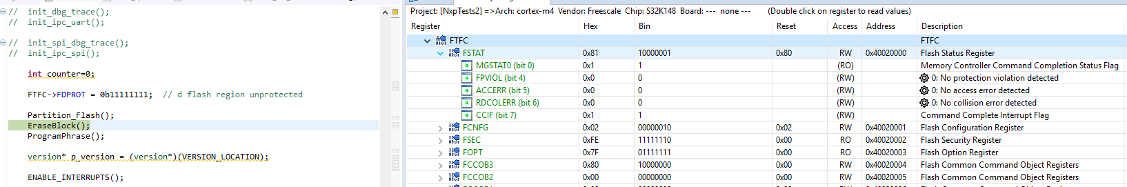
My problem is, that when I try to erase a flash block, I can see the access error bit set in status register of the flash controler. As I switched off memory protection (I set FTFC->FDPROT = 0b11111111; before I call my method Partition_Flash; compare to section 36.4.4.1.9 in chips reference manual) and used an address relative to the start of the flash partition, I do not understand, how this could lead to access error situations.
Here are some details on my problem.
My approach to achieve this goal is:
- Partition the flash
- Erase a flash block
- Write data using the program phrase command
My clock settings are: 160 MHz SPLL, 80 MHz core clock, 40 MHz bus clock, 26,6 MHz flash clock.
This is how I partition the flash area:
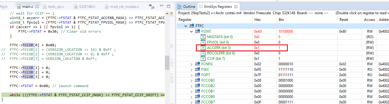
void Partition_Flash() {
while (((FTFC->FSTAT & FTFC_FSTAT_CCIF_MASK) >> FTFC_FSTAT_CCIF_SHIFT) == 0)
;
// wait for CCIF == 1
uint8_t accerr = (FTFC->FSTAT & FTFC_FSTAT_ACCERR_MASK) >> FTFC_FSTAT_ACCERR_SHIFT;
uint8_t fpviol = (FTFC->FSTAT & FTFC_FSTAT_FPVIOL_MASK)
>> FTFC_FSTAT_FPVIOL_SHIFT;
if (accerr == 1 || fpviol == 1) {
FTFC->FSTAT = 0x30; // Clear old errors
}
// partition flash: see 36.5.11.14 Program Partition command p838ff RM
FTFC->FCCOB[0] = 0x80;
FTFC->FCCOB[1] = 0x0;
FTFC->FCCOB[2] = 0x0;
FTFC->FCCOB[3] = 0x1;
FTFC->FCCOB[4] = 0xF;
FTFC->FCCOB[5] = 0;
FTFC->FSTAT = 0x80; // launch command
while (((FTFC->FSTAT & FTFC_FSTAT_CCIF_MASK) >> FTFC_FSTAT_CCIF_SHIFT) == 0)
;
// wait for CCIF == 1
}When debugging, the register view in S32 Design Studio does not show any error after the partition command has been executed.

Next step is to erase a flash block using the following code:
void EraseBlock()
{
// Erase flash block
while (((FTFC->FSTAT & FTFC_FSTAT_CCIF_MASK) >> FTFC_FSTAT_CCIF_SHIFT) == 0);
// wait for CCIF == 1
uint8_t accerr = (FTFC->FSTAT & FTFC_FSTAT_ACCERR_MASK) >> FTFC_FSTAT_ACCERR_SHIFT;
uint8_t fpviol = (FTFC->FSTAT & FTFC_FSTAT_FPVIOL_MASK) >> FTFC_FSTAT_FPVIOL_SHIFT;
if (accerr == 1 || fpviol == 1) {
FTFC->FSTAT = 0x30; // Clear old errors
}
FTFC->FCCOB[0] = 0x08;
// from my understanding this should be the first flash block
FTFC->FCCOB[1] = 0;
FTFC->FCCOB[2] = 0;
FTFC->FCCOB[3] = 0;
FTFC->FSTAT = 0x80; // launch command
while (((FTFC->FSTAT & FTFC_FSTAT_CCIF_MASK) >> FTFC_FSTAT_CCIF_SHIFT) == 0);
}Howver, right after writing value 0x80 into FTFC->FSTAT, in the register view the access error bit in register FSTAT is set.

Now my questions are
- Why does the access error occur?
- Is there any step missing in my approach?
Any help would be appreciated.
Best Regards,
Michael
Solved! Go to Solution.
- Mark as New
- Bookmark
- Subscribe
- Mute
- Subscribe to RSS Feed
- Permalink
- Report Inappropriate Content
Hello Michael,
As you can see in Section 36.5.11 RM rev.9
When required by the command, address bit 23 selects between program flash memory (=0) and data flash memory (=1).
FTFC->FCCOB[3] = 0x08; // FCCOB0 ERSBLK
FTFC->FCCOB[2] = 0x80; // Flash address [23:16] of 0x1000_0000
FTFC->FCCOB[1] = 0x00; // Flash address [15:8]
FTFC->FCCOB[1] = 0x00; // Flash address [7:0]Regards,
Daniel
- Mark as New
- Bookmark
- Subscribe
- Mute
- Subscribe to RSS Feed
- Permalink
- Report Inappropriate Content
Hello Daniel,
I found this comment in the RM, so thank you for this hint.
Your code snippet works for me, only three more questions on that topic:
- Line 4 of your snippet should be FTFC->FCCOB[0] = 0x0, correct?
- RM section 36.4.4.1.6.4 Fields states "The individual registers that compose the FCCOB data set can be written in any order, but you must provide all needed values, which vary from command to command." But you start to compose the command by writing FCCOB3 first. Is this because of the offsets stated in RM section 36.4.4.1.6.1 Offset ?
- Does the command byte always go to FTFC->FCCOB[3]? In the command descriptions the command byte is always mentioned to be written in FCCOB Number 0. This confuses me a bit.
Best Regards,
Michael
- Mark as New
- Bookmark
- Subscribe
- Mute
- Subscribe to RSS Feed
- Permalink
- Report Inappropriate Content
Hello Michael,
1. Sorry, just a typo.
2. It really does not matter.
3. It is FCCOB0 which is offset by 3, that means FTFC->FCCOB[3]. Yes, it is confusing.
BR, Daniel