
- Forums
- Product Forums
- General Purpose MicrocontrollersGeneral Purpose Microcontrollers
- i.MX Forumsi.MX Forums
- QorIQ Processing PlatformsQorIQ Processing Platforms
- Identification and SecurityIdentification and Security
- Power ManagementPower Management
- MCX Microcontrollers
- S32G
- S32K
- S32V
- MPC5xxx
- Other NXP Products
- Wireless Connectivity
- S12 / MagniV Microcontrollers
- Powertrain and Electrification Analog Drivers
- Sensors
- Vybrid Processors
- Digital Signal Controllers
- 8-bit Microcontrollers
- ColdFire/68K Microcontrollers and Processors
- PowerQUICC Processors
- OSBDM and TBDML
-
- Solution Forums
- Software Forums
- MCUXpresso Software and ToolsMCUXpresso Software and Tools
- CodeWarriorCodeWarrior
- MQX Software SolutionsMQX Software Solutions
- Model-Based Design Toolbox (MBDT)Model-Based Design Toolbox (MBDT)
- FreeMASTER
- eIQ Machine Learning Software
- Embedded Software and Tools Clinic
- S32 SDK
- S32 Design Studio
- GUI Guider
- Zephyr Project
- Voice Technology
- Application Software Packs
- Secure Provisioning SDK (SPSDK)
- Processor Expert Software
- MCUXpresso Training Hub
-
- Topics
- Mobile Robotics - Drones and RoversMobile Robotics - Drones and Rovers
- NXP Training ContentNXP Training Content
- University ProgramsUniversity Programs
- Rapid IoT
- NXP Designs
- SafeAssure-Community
- OSS Security & Maintenance
- Using Our Community
-
- Cloud Lab Forums
-
- Knowledge Bases
- ARM Microcontrollers
- i.MX Processors
- Identification and Security
- Model-Based Design Toolbox (MBDT)
- QorIQ Processing Platforms
- S32 Automotive Processing Platform
- Wireless Connectivity
- CodeWarrior
- MCUXpresso Suite of Software and Tools
- MQX Software Solutions
-
- Home
- :
- Product Forums
- :
- S32K
- :
- S32K144 LPSPI0 GD25P16 Flash slave no MISO response
S32K144 LPSPI0 GD25P16 Flash slave no MISO response
- Subscribe to RSS Feed
- Mark Topic as New
- Mark Topic as Read
- Float this Topic for Current User
- Bookmark
- Subscribe
- Mute
- Printer Friendly Page
S32K144 LPSPI0 GD25P16 Flash slave no MISO response
- Mark as New
- Bookmark
- Subscribe
- Mute
- Subscribe to RSS Feed
- Permalink
- Report Inappropriate Content
I am using an external flash memory called GD25P16, with a S32K144 microcontroler and i am trying to make them communicate through a LPSPI0 bus.
my problem is, I have no response from the GD25P16 on my requests.And Flash HOLD pin and WP pin is directly connected 3.3v.
My LPSPI0 Configuration is
CS : GPIO_PTB5 PCS1 MUX3
MOSI: GPIO_PTB4 MUX3
MISO: GPIO_PTB3 MUX3
CLK: GPIO_PTB2 MUX3
////////////////////////////////////////////////////////////LPSPI Pin config//////////////////////////////////////////////////////////////
pin_settings_config_t g_pin_mux_InitConfigArr_SPI0[4] = {
{
.base = PORTB,
.pinPortIdx = 2u,
.pullConfig = PORT_INTERNAL_PULL_NOT_ENABLED,
.passiveFilter = false,
.driveSelect = PORT_LOW_DRIVE_STRENGTH,
.mux = PORT_MUX_ALT3,
.pinLock = false,
.intConfig = PORT_DMA_INT_DISABLED,
.clearIntFlag = false,
.gpioBase = NULL,
},
{
.base = PORTB,
.pinPortIdx = 3u,
.pullConfig = PORT_INTERNAL_PULL_NOT_ENABLED,
.passiveFilter = false,
.driveSelect = PORT_LOW_DRIVE_STRENGTH,
.mux = PORT_MUX_ALT3,
.pinLock = false,
.intConfig = PORT_DMA_INT_DISABLED,
.clearIntFlag = false,
.gpioBase = NULL,
},
{
.base = PORTB,
.pinPortIdx = 4u,
.pullConfig = PORT_INTERNAL_PULL_NOT_ENABLED,
.passiveFilter = false,
.driveSelect = PORT_LOW_DRIVE_STRENGTH,
.mux = PORT_MUX_ALT3,
.pinLock = false,
.intConfig = PORT_DMA_INT_DISABLED,
.clearIntFlag = false,
.gpioBase = NULL,
},
{
.base = PORTB,
.pinPortIdx = 5u,
.pullConfig = PORT_INTERNAL_PULL_NOT_ENABLED,
.passiveFilter = false,
.driveSelect = PORT_LOW_DRIVE_STRENGTH,
.mux = PORT_MUX_ALT3,
.pinLock = false,
.intConfig = PORT_DMA_INT_DISABLED,
.clearIntFlag = false,
.gpioBase = NULL,
},
};
//////////////////////////////////////////////////////////////////////////////////////////////////////////////////////////////////////////////////////////
void LPSPI0_Init(void)
{
const lpspi_master_config_t Send_MasterConfig0 =
{
.bitsPerSec = 500000U,
.whichPcs = LPSPI_PCS1,
.pcsPolarity = LPSPI_ACTIVE_LOW,
.isPcsContinuous = false,
.bitcount = 8U,
.lpspiSrcClk = 48000000U,
.clkPhase = LPSPI_CLOCK_PHASE_2ND_EDGE,
.clkPolarity = LPSPI_SCK_ACTIVE_LOW,
.lsbFirst = false,
.transferType = LPSPI_USING_INTERRUPTS,
.rxDMAChannel = 255,
.txDMAChannel = 255,
.callback = lpspi0_callback,
.callbackParam = NULL,
};
PCC->PCCn[PCC_PORTB_INDEX] |= PCC_PCCn_CGC_MASK; /* Enable clock for PORTB */
PCC->PCCn[PCC_LPSPI0_INDEX] = 0; /* Disable clocks to modify PCS ( default) */
PCC->PCCn[PCC_LPSPI0_INDEX] = 0xC6000000; /* Enable PCS=SPLL_DIV2 */
PINS_DRV_Init(4, g_pin_mux_InitConfigArr_SPI0);
lpspistate.callback = lpspi0_callback;
LPSPI_DRV_MasterInit(0, &lpspistate, &Send_MasterConfig0);
LPSPI_DRV_MasterSetDelay(0, 1, 1, 1);
}

I connected the logic analyzer to the chip and i can see SPI signals being generated by the MCU and to me they seem correct.But MISO Pin is always no signal.(MISO PIN is not shorted and isn't used by other)
This is S32K and Flash logic analyzer

I try connected Flash SPI 4 PIN to STM32 microcontroler. Unexpectedly, Flash has response. The SCK Clock goes the same 500KHz.
This is STM32 and Flash logic analyzer.

I can't find anything on the web to help me so if someone have a solution to this problem, please help me, you are really welcome here ! thanks.
- Mark as New
- Bookmark
- Subscribe
- Mute
- Subscribe to RSS Feed
- Permalink
- Report Inappropriate Content
/*
* SPI_FLASH_WRITE_READ
* SPI FLASH : MX25L16xx
* Author : wjandsq@163.com
* Date : 2020/06/28
* Historys : 2020/07/21 fixed some bugs
* 2020/07/22 SPI FLASH Page Pragram 256 bytes is OK (Wrirt and Read 260 bytes)
*/
void SPI_FLASH_WRITE_READ(uint8_t *txdata_p, uint8_t * rxdata_p, uint16_t size)
{
uint32_t words;
uint32_t remain_words;
uint32_t remain_bytes;
uint32_t lpspi_tmp;
uint32_t lpspi_tmp2;
LPSPI1->CFGR1 = 0x00000003; /* MASTER、SAMPLE Set */
LPSPI1->FCR = 0x00000003; /* RXWATER=0 TXWATER=3 */
LPSPI1->CR = 0x00000009; /* Module Enable、Debug Enable */
LPSPI1->TCR = ((LPSPI1->TCR) & ~(LPSPI_TCR_CONTC_MASK | LPSPI_TCR_TXMSK_MASK | LPSPI_TCR_RXMSK_MASK));
if (size % 4) {
remain_bytes = size - (size / 4) * 4;
words = (size / 4) + 1;
} else {
remain_bytes = 0;
words = size / 4;
}
remain_words = words;
/* When SPI FLASH Page Program Write, n = 1, 2, 3.... 64, 65
* size = 256 + 4
* word = 260 / 4 = 65
*/
if (size % 4 == 0) {
/* size is 4 bytes * n (n = 1 2 3 ... n) */
lpspi_tmp = ((LPSPI1->TCR) & (~LPSPI_TCR_FRAMESZ_MASK));
LPSPI1->TCR = (lpspi_tmp | (31U & LPSPI_TCR_FRAMESZ_MASK));
PINS_DRV_ClearPins(PTB, 1 << 17); /*<! Software Control PCS3 : SET PCS3 LOW */
for (i = 0; i < words; ++i) {
/* between word delay 3.8 us, between 4 words delay is 5us */
while (((LPSPI1->SR & LPSPI_SR_TDF_MASK) >> LPSPI_SR_TDF_SHIFT) == 0);
LPSPI1->TDR = (*( const uint32_t * ) (txdata_p));
LPSPI1->TCR = ((LPSPI1->TCR) | (LPSPI_TCR_TXMSK_MASK)); /*<! Start Transmit and Hardware Auto Clear */
LPSPI1->TCR = ((LPSPI1->TCR) & (~LPSPI_TCR_RXMSK_MASK));
LPSPI1->SR = LPSPI_SR_TDF_MASK; /*<! Clear TDF flag */
txdata_p = txdata_p + 4;
while (((LPSPI1->SR & LPSPI_SR_RDF_MASK) >> LPSPI_SR_RDF_SHIFT) == 0);
(*( uint32_t * ) (rxdata_p)) = LPSPI1->RDR;
LPSPI1->SR = LPSPI_SR_RDF_MASK; /*<! Clear RDF flag */
rxdata_p = rxdata_p + 4;
}
while (((LPSPI1->SR & LPSPI_SR_FCF_MASK) >> LPSPI_SR_FCF_SHIFT) == 0);
LPSPI1->SR |= LPSPI_SR_FCF_MASK; /*<! Clear FCF flag */
PINS_DRV_SetPins(PTB, 1 << 17); /*<! Software Control PCS3 : SET PCS3 High */
LPSPI1->CR = 0x00000000; /*<! Module Disable、Debug Disable */
return;
}
if (size == 1) {
/* send data size is 1 byte */
lpspi_tmp = ((LPSPI1->TCR) & (~LPSPI_TCR_FRAMESZ_MASK));
LPSPI1->TCR = (lpspi_tmp | (7U & LPSPI_TCR_FRAMESZ_MASK));
PINS_DRV_ClearPins(PTB, 1 << 17); /*<! Software Control PCS3 : SET PCS3 LOW */
.
.
.
PINS_DRV_SetPins(PTB, 1 << 17); /*<! Software Control PCS3 : SET PCS3 High */
} else if (size == 2) {
/* send data size is 2 bytes */
lpspi_tmp = ((LPSPI1->TCR) & (~LPSPI_TCR_FRAMESZ_MASK));
LPSPI1->TCR = (lpspi_tmp | (15U & LPSPI_TCR_FRAMESZ_MASK));
PINS_DRV_ClearPins(PTB, 1 << 17); /*<! Software Control PCS3 : SET PCS3 LOW */
.
.
.
PINS_DRV_SetPins(PTB, 1 << 17); /*<! Software Control PCS3 : SET PCS3 High */
} else if (size == 3) {
/* send data size is 3 bytes */
lpspi_tmp = ((LPSPI1->TCR) & (~LPSPI_TCR_FRAMESZ_MASK));
LPSPI1->TCR = (lpspi_tmp | (23U & LPSPI_TCR_FRAMESZ_MASK));
PINS_DRV_ClearPins(PTB, 1 << 17); /*<! Software Control PCS3 : SET PCS3 LOW */
.
.
.
PINS_DRV_SetPins(PTB, 1 << 17); /*<! Software Control PCS3 : SET PCS3 High */
} else {
/* send data size is 5、6、7 bytes or size > 8 bytes */
lpspi_tmp = ((LPSPI1->TCR) & (~LPSPI_TCR_FRAMESZ_MASK));
LPSPI1->TCR = (lpspi_tmp | (31U & LPSPI_TCR_FRAMESZ_MASK));
PINS_DRV_ClearPins(PTB, 1 << 17); /* Software Control PCS3 : SET PCS3 LOW */
for (uint16_t i = 0; i < words; ) {
if (remain_words > 2) {
/* send data size > 8 bytes */
.
.
.
--remain_words;
++i;
} else if (remain_words == 2) {
/* send data size is 5、6、7 bytes */
lpspi_tmp = remain_bytes * 8 + 31;
lpspi_tmp2 = ((LPSPI1->TCR) & (~LPSPI_TCR_FRAMESZ_MASK));
LPSPI1->TCR = (lpspi_tmp2 | (lpspi_tmp & LPSPI_TCR_FRAMESZ_MASK));
.
.
.
remain_words = remain_words - 2;
i = i + 2;
}
}
PINS_DRV_SetPins(PTB, 1 << 17); /*<! Software Control PCS3 : SET PCS3 High */
}
}
- Mark as New
- Bookmark
- Subscribe
- Mute
- Subscribe to RSS Feed
- Permalink
- Report Inappropriate Content
Hi 935367276@qq.com,
Please see the CS signal.
The S32K144 MCU de-asserts the CS after each 8-bit frame.


The GD25P16 probably requires 32-bit or 40-bit frames.
Regards,
Daniel
- Mark as New
- Bookmark
- Subscribe
- Mute
- Subscribe to RSS Feed
- Permalink
- Report Inappropriate Content


If the transmitted bytes exceed 16 bytes (4 WORD), NXP cannot provide a useful LPSPI program, and there are too many bugs about LPSPI. Especially, PCS cannot be controlled by software.
For STM32F4, without interrupt and DMA, the following code can achieve full duplex. But there is no way for S32K144.
/* for 40MHz SPI */
uint8_t RxData;
while((hspi->Instance->SR & SPI_SR_TXE) != SPI_SR_TXE);
*((__IO uint8_t *)&hspi->Instance->DR) = TxData;
while((hspi->Instance->SR & SPI_SR_RXNE) != SPI_SR_RXNE);
RxData = *((__IO uint8_t *)&hspi->Instance->DR);
return RxData;
- Mark as New
- Bookmark
- Subscribe
- Mute
- Subscribe to RSS Feed
- Permalink
- Report Inappropriate Content
Hello wjandsq,
Although the FIFOs are 4-word long, the LPSPI can transmit more than that in a single frame, this is configurable by the FRAMESZ bit field in the TCR transmit command registers.
Or you can use the continues transfer feature TCR_CONT = 1, then, the PCS stays asserted between frames.
You can also emulated PCS by SW, please have a look at the Status Register, you can use the TCF, FCF flags.
The SDK has a LPSPI driver and there is an example as well (lpspi_transfer_s32k144).
Regards,
Daniel
- Mark as New
- Bookmark
- Subscribe
- Mute
- Subscribe to RSS Feed
- Permalink
- Report Inappropriate Content
void spi_simple_bytes_wr(uint8_t *txdata_p, uint8_t * rxdata_p, uint8_t size)
{
uint32_t lpspi_tmp;
uint32_t lpspi_tmp2;
uint8_t i;
uint8_t remain_size = size;
if (size == 1) {
/* 2020/07/01 SPI FLASH Sequence for 1 bytes is OK */
LPSPI1->TCR = ((LPSPI1->TCR) & (~LPSPI_TCR_BYSW_MASK));
LPSPI1->FCR = 0x00000003; /* RXWATER=0 TXWATER=3 */
lpspi_tmp = ((LPSPI1->TCR) & (~LPSPI_TCR_FRAMESZ_MASK));
LPSPI1->TCR = (lpspi_tmp | (7U & LPSPI_TCR_FRAMESZ_MASK));
PINS_DRV_ClearPins(PTB, 1 << 17); /* Software Control PCS3 : SET PCS3 LOW */
while (((LPSPI1->SR & LPSPI_SR_TDF_MASK) >> LPSPI_SR_TDF_SHIFT) == 0);
LPSPI1->TDR = ( uint32_t ) (*txdata_p++);
LPSPI1->TCR = ((LPSPI1->TCR) | (LPSPI_TCR_TXMSK_MASK)); /* Start Transmit and Hardware Auto Clear */
LPSPI1->TCR = ((LPSPI1->TCR) & (~LPSPI_TCR_RXMSK_MASK));
LPSPI1->SR |= LPSPI_SR_TDF_MASK; /* Clear TDF flag */
while (((LPSPI1->SR & LPSPI_SR_RDF_MASK) >> LPSPI_SR_RDF_SHIFT) == 0);
lpspi_tmp = LPSPI1->RDR;
*rxdata_p++ = ( uint8_t ) (lpspi_tmp >> 24);
while (((LPSPI1->SR & LPSPI_SR_FCF_MASK) >> LPSPI_SR_FCF_SHIFT) == 0);
LPSPI1->SR |= LPSPI_SR_RDF_MASK | LPSPI_SR_FCF_MASK;
LPSPI1->TCR = ((LPSPI1->TCR) & (~LPSPI_TCR_CONTC_MASK));
LPSPI1->CR = 0x00000000; /* Module Disable、Debug Disable */
PINS_DRV_SetPins(PTB, 1 << 17); /* Software Control PCS3 : SET PCS3 High */
} else if (size == 2) {
/* 2020/07/01 SPI FLASH Sequence for 2 bytes */
LPSPI1->TCR = ((LPSPI1->TCR) & (~LPSPI_TCR_BYSW_MASK));
LPSPI1->FCR = 0x00000003; /* RXWATER=0 TXWATER=3 */
lpspi_tmp = ((LPSPI1->TCR) & (~LPSPI_TCR_FRAMESZ_MASK));
LPSPI1->TCR = (lpspi_tmp | (15U & LPSPI_TCR_FRAMESZ_MASK));
lpspi_tmp = (*txdata_p++);
lpspi_tmp = lpspi_tmp << 8;
lpspi_tmp |= (*txdata_p++);
PINS_DRV_ClearPins(PTB, 1 << 17); /* Software Control PCS3 : SET PCS3 LOW */
while (((LPSPI1->SR & LPSPI_SR_TDF_MASK) >> LPSPI_SR_TDF_SHIFT) == 0);
LPSPI1->TDR = lpspi_tmp;
LPSPI1->TCR = ((LPSPI1->TCR) | (LPSPI_TCR_TXMSK_MASK)); /* Start Transmit and Hardware Auto Clear */
LPSPI1->TCR = ((LPSPI1->TCR) & (~LPSPI_TCR_RXMSK_MASK));
LPSPI1->SR |= LPSPI_SR_TDF_MASK; /* Clear TDF flag */
while (((LPSPI1->SR & LPSPI_SR_RDF_MASK) >> LPSPI_SR_RDF_SHIFT) == 0);
lpspi_tmp = LPSPI1->RDR;
while (((LPSPI1->SR & LPSPI_SR_FCF_MASK) >> LPSPI_SR_FCF_SHIFT) == 0);
LPSPI1->SR |= LPSPI_SR_RDF_MASK | LPSPI_SR_FCF_MASK;
LPSPI1->TCR = ((LPSPI1->TCR) & (~LPSPI_TCR_CONTC_MASK));
LPSPI1->CR = 0x00000000; /* Module Disable、Debug Disable */
PINS_DRV_SetPins(PTB, 1 << 17); /* Software Control PCS3 : SET PCS3 High */
*rxdata_p++ = ( uint8_t ) ((lpspi_tmp >> 16) & 0x000000FF);
*rxdata_p++ = ( uint8_t ) ((lpspi_tmp >> 24) & 0x000000FF);
} else if (size == 3) {
/* 2020/07/01 SPI FLASH Sequence for 3 bytes is OK */
LPSPI1->TCR = ((LPSPI1->TCR) & (~LPSPI_TCR_BYSW_MASK));
LPSPI1->FCR = 0x00000003; /* RXWATER=0 TXWATER=3 */
lpspi_tmp = ((LPSPI1->TCR) & (~LPSPI_TCR_FRAMESZ_MASK));
LPSPI1->TCR = (lpspi_tmp | (23U & LPSPI_TCR_FRAMESZ_MASK));
lpspi_tmp = (*txdata_p++);
lpspi_tmp = lpspi_tmp << 8;
lpspi_tmp |= (*txdata_p++);
lpspi_tmp = lpspi_tmp << 8;
lpspi_tmp |= (*txdata_p++);
PINS_DRV_ClearPins(PTB, 1 << 17); /* Software Control PCS3 : SET PCS3 LOW */
while (((LPSPI1->SR & LPSPI_SR_TDF_MASK) >> LPSPI_SR_TDF_SHIFT) == 0);
LPSPI1->TDR = lpspi_tmp;
LPSPI1->TCR = ((LPSPI1->TCR) | (LPSPI_TCR_TXMSK_MASK)); /* Start Transmit and Hardware Auto Clear */
LPSPI1->TCR = ((LPSPI1->TCR) & (~LPSPI_TCR_RXMSK_MASK));
LPSPI1->SR |= LPSPI_SR_TDF_MASK; /* Clear TDF flag */
while (((LPSPI1->SR & LPSPI_SR_RDF_MASK) >> LPSPI_SR_RDF_SHIFT) == 0);
lpspi_tmp = LPSPI1->RDR;
while (((LPSPI1->SR & LPSPI_SR_FCF_MASK) >> LPSPI_SR_FCF_SHIFT) == 0);
LPSPI1->SR |= LPSPI_SR_RDF_MASK | LPSPI_SR_FCF_MASK;
LPSPI1->TCR = ((LPSPI1->TCR) & (~LPSPI_TCR_CONTC_MASK));
LPSPI1->CR = 0x00000000; /* Module Disable、Debug Disable */
PINS_DRV_SetPins(PTB, 1 << 17); /* Software Control PCS3 : SET PCS3 High */
*rxdata_p++ = ( uint8_t ) ((lpspi_tmp >> 8) & 0x000000FF);
*rxdata_p++ = ( uint8_t ) ((lpspi_tmp >> 16) & 0x000000FF);
*rxdata_p++ = ( uint8_t ) ((lpspi_tmp >> 24) & 0x000000FF);
} else if (size == 4) {
/* 4 bytes Transmit and Receive */
/* 2020/07/01 SPI FLASH Read_Identification_Sequence for 4 bytes is OK */
// LPSPI1->TCR = ((LPSPI1->TCR) & (~LPSPI_TCR_BYSW_MASK));
LPSPI1->TCR = ((LPSPI1->TCR) | (LPSPI_TCR_BYSW_MASK));
LPSPI1->FCR = 0x00000002; /* RXWATER=0 TXWATER=2 */
lpspi_tmp = ((LPSPI1->TCR) & (~LPSPI_TCR_FRAMESZ_MASK));
LPSPI1->TCR = (lpspi_tmp | (31 & LPSPI_TCR_FRAMESZ_MASK));
lpspi_tmp = ( uint32_t ) (*( const uint32_t * ) (txdata_p));
PINS_DRV_ClearPins(PTB, 1 << 17); /* Software Control PCS3 : SET PCS3 LOW */
while (((LPSPI1->SR & LPSPI_SR_TDF_MASK) >> LPSPI_SR_TDF_SHIFT) == 0);
LPSPI1->TDR = lpspi_tmp;
LPSPI1->TCR = ((LPSPI1->TCR) | (LPSPI_TCR_TXMSK_MASK)); /* Start Transmit and Hardware Auto Clear */
LPSPI1->TCR = ((LPSPI1->TCR) & (~LPSPI_TCR_RXMSK_MASK));
LPSPI1->SR |= LPSPI_SR_TDF_MASK; /* Clear TDF flag */
while (((LPSPI1->SR & LPSPI_SR_RDF_MASK) >> LPSPI_SR_RDF_SHIFT) == 0);
lpspi_tmp = LPSPI1->RDR;
LPSPI1->CR = 0x00000000; /* Module Disable、Debug Disable */
PINS_DRV_SetPins(PTB, 1 << 17); /* Software Control PCS3 : SET PCS3 High */
LPSPI1->TCR = ((LPSPI1->TCR) & (~LPSPI_TCR_CONTC_MASK));
/* Big end Receive, store is Little end */
*rxdata_p++ = ( uint8_t ) ((lpspi_tmp >> 0) & 0x000000FF);
*rxdata_p++ = ( uint8_t ) ((lpspi_tmp >> 8) & 0x000000FF);
*rxdata_p++ = ( uint8_t ) ((lpspi_tmp >> 16) & 0x000000FF);
*rxdata_p++ = ( uint8_t ) ((lpspi_tmp >> 24) & 0x000000FF);
} else {
if ((size > 5) && (size <= 8)) {
/* Clean RX and TX buffers */
lpspi_tmp = (0x01 << LPSPI_CR_RRF_SHIFT) | (0x01 << LPSPI_CR_RTF_SHIFT);
LPSPI1->CR |= lpspi_tmp;
/* The second flush command is used to avoid the case when one word is still in shifter. */
lpspi_tmp = (0x01 << LPSPI_CR_RRF_SHIFT) | (0x01 << LPSPI_CR_RTF_SHIFT);
LPSPI1->CR |= lpspi_tmp;
/* 5 bytes to 8 bytes Transmit and Receive (Frame_Size 40bit、 48bit、 56bit、64bit) */
lpspi_tmp = size * 8 - 1;
LPSPI1->TCR = ((LPSPI1->TCR) | (LPSPI_TCR_BYSW_MASK));
LPSPI1->TCR = ((LPSPI1->TCR) & (~LPSPI_TCR_TXMSK_MASK));
LPSPI1->TCR = ((LPSPI1->TCR) & (~LPSPI_TCR_RXMSK_MASK));
lpspi_tmp2 = ((LPSPI1->TCR) & (~LPSPI_TCR_FRAMESZ_MASK));
LPSPI1->TCR = (lpspi_tmp2 | ((lpspi_tmp) & LPSPI_TCR_FRAMESZ_MASK));
LPSPI1->SR |= 0x00003F00U;
lpspi_tmp = (*( const uint32_t * ) (txdata_p));
txdata_p = txdata_p + 4;
lpspi_tmp2 = (*( const uint32_t * ) (txdata_p));
txdata_p = txdata_p + 4;
while (((LPSPI1->SR & LPSPI_SR_TDF_MASK) >> LPSPI_SR_TDF_SHIFT) == 0);
LPSPI1->TDR = lpspi_tmp;
LPSPI1->TDR = lpspi_tmp2;
LPSPI1->SR = LPSPI_SR_TDF_MASK; /* Clear TDF flag */
LPSPI1->TCR = ((LPSPI1->TCR) | (LPSPI_TCR_TXMSK_MASK));
LPSPI1->TCR = ((LPSPI1->TCR) & (~LPSPI_TCR_RXMSK_MASK));
while (((LPSPI1->SR & LPSPI_SR_RDF_MASK) >> LPSPI_SR_RDF_SHIFT) == 0);
lpspi_tmp = LPSPI1->RDR;
LPSPI1->SR = LPSPI_SR_RDF_MASK; /* Clear RDF flag */
while (((LPSPI1->SR & LPSPI_SR_RDF_MASK) >> LPSPI_SR_RDF_SHIFT) == 0);
lpspi_tmp2 = LPSPI1->RDR;
while (((LPSPI1->SR & LPSPI_SR_FCF_MASK) >> LPSPI_SR_FCF_SHIFT) == 0);
LPSPI1->SR |= LPSPI_SR_RDF_MASK; /* Clear RDF flag */
PINS_DRV_SetPins(PTB, 1 << 17); /* Software Control PCS3 : SET PCS3 High */
LPSPI1->CR = 0x00000000; /* Module Disable、Debug Disable */
/* Big end Receive, store is Little end */
*rxdata_p++ = ( uint8_t ) ((lpspi_tmp >> 0) & 0x000000FF);
*rxdata_p++ = ( uint8_t ) ((lpspi_tmp >> 8) & 0x000000FF);
*rxdata_p++ = ( uint8_t ) ((lpspi_tmp >> 16) & 0x000000FF);
*rxdata_p++ = ( uint8_t ) ((lpspi_tmp >> 24) & 0x000000FF);
remain_size = size - 4;
for (i = 0; i < remain_size; ++i) {
*(rxdata_p + remain_size - 1 - i) = ( uint8_t ) (lpspi_tmp2 >> (24 - i * 8));
}
} else if ((size > 8) && (size <= 16)) {
// test is OK
} else if ((size > 16)) {
// is OK ?
}
}
}
NXP have a SPI Write and Read example for SPI FLASH ? the SPI1 interrupt SDK is up 40Mbps ?
- Mark as New
- Bookmark
- Subscribe
- Mute
- Subscribe to RSS Feed
- Permalink
- Report Inappropriate Content
Hello wjandsq,
I have just gone through the code briefly and I see one possible issue.
The Transmit Command Register (TCR) is not an ordinary register but a FIFO.
Please don't mask the register but prepare your transmit commands in variables (or use constants) and write the whole register at once whenever you need to change it.
There are these LPSPI SDK examples:
- lpspi_dma_s32k144
- lpspi_transfer_s32k144
The LPSPI max baud rate (Frequency of operation) is specified in the S32K1xx datasheet.
https://www.nxp.com/docs/en/data-sheet/S32K-DS.pdf
Table 46. LPSPI electrical specifications
BR, Daniel
- Mark as New
- Bookmark
- Subscribe
- Mute
- Subscribe to RSS Feed
- Permalink
- Report Inappropriate Content
I don't need an interrupt example or DMA example, they can work, but they always make mistakes.
Now , Either TDFor TDF , it is impossible to judge when the data has been sent finished.
1 to 16 byte , the pcs3 is ok, but > 16 bytes, the pcs3 always error,before data finishe, the pcs trun high。
- Mark as New
- Bookmark
- Subscribe
- Mute
- Subscribe to RSS Feed
- Permalink
- Report Inappropriate Content
Could you please describe what exactly you want to achieve?
And why do you need to control CS by GPIO?
S32K144:SPI Transfer with GPIO as CS
Thanks,
BR, Daniel
- Mark as New
- Bookmark
- Subscribe
- Mute
- Subscribe to RSS Feed
- Permalink
- Report Inappropriate Content
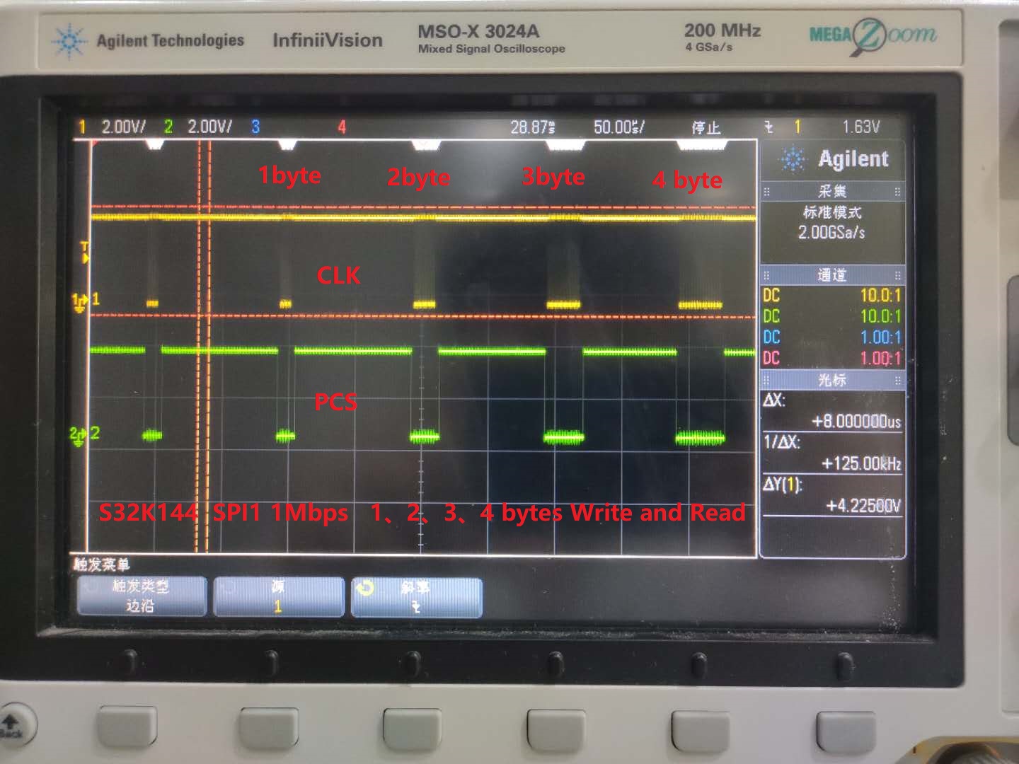
The SPI FLASH PCS need keep Low when Read or Write 260 bytes (or Write 1、2、3、4、5、6 bytes Command)。
- Mark as New
- Bookmark
- Subscribe
- Mute
- Subscribe to RSS Feed
- Permalink
- Report Inappropriate Content
Hi,
I modified the lpspi_transfer_s32k144 SDK example to send and receive 260 bytes continuously without deasserting the PCS PTB0 (active high).
The LPSPI slave was removed from the project.
Connect PTB4 (MOSI) to PTE1 (MISO) so that the master can receive that transmitted data back.
We don't have any non-SDK LPSPI example that would shows continuous transfer.
BR, Daniel
- Mark as New
- Bookmark
- Subscribe
- Mute
- Subscribe to RSS Feed
- Permalink
- Report Inappropriate Content
Thanks a lot! but my code is in 10Mbps or 20Mbps without DMA and interrupt. Write and Read NOR FLASH 256 bytes (260 bytes)test is OK.