- Forums
- Product Forums
- General Purpose MicrocontrollersGeneral Purpose Microcontrollers
- i.MX Forumsi.MX Forums
- QorIQ Processing PlatformsQorIQ Processing Platforms
- Identification and SecurityIdentification and Security
- Power ManagementPower Management
- Wireless ConnectivityWireless Connectivity
- RFID / NFCRFID / NFC
- Advanced AnalogAdvanced Analog
- MCX Microcontrollers
- S32G
- S32K
- S32V
- MPC5xxx
- Other NXP Products
- S12 / MagniV Microcontrollers
- Powertrain and Electrification Analog Drivers
- Sensors
- Vybrid Processors
- Digital Signal Controllers
- 8-bit Microcontrollers
- ColdFire/68K Microcontrollers and Processors
- PowerQUICC Processors
- OSBDM and TBDML
- S32M
- S32Z/E
-
- Solution Forums
- Software Forums
- MCUXpresso Software and ToolsMCUXpresso Software and Tools
- CodeWarriorCodeWarrior
- MQX Software SolutionsMQX Software Solutions
- Model-Based Design Toolbox (MBDT)Model-Based Design Toolbox (MBDT)
- FreeMASTER
- eIQ Machine Learning Software
- Embedded Software and Tools Clinic
- S32 SDK
- S32 Design Studio
- GUI Guider
- Zephyr Project
- Voice Technology
- Application Software Packs
- Secure Provisioning SDK (SPSDK)
- Processor Expert Software
- Generative AI & LLMs
-
- Topics
- Mobile Robotics - Drones and RoversMobile Robotics - Drones and Rovers
- NXP Training ContentNXP Training Content
- University ProgramsUniversity Programs
- Rapid IoT
- NXP Designs
- SafeAssure-Community
- OSS Security & Maintenance
- Using Our Community
-
- Cloud Lab Forums
-
- Knowledge Bases
- ARM Microcontrollers
- i.MX Processors
- Identification and Security
- Model-Based Design Toolbox (MBDT)
- QorIQ Processing Platforms
- S32 Automotive Processing Platform
- Wireless Connectivity
- CodeWarrior
- MCUXpresso Suite of Software and Tools
- MQX Software Solutions
- RFID / NFC
- Advanced Analog
-
- NXP Tech Blogs
- Home
- :
- Product Forums
- :
- S12 / MagniV Microcontrollers Knowledge Base
- :
- S12ZVM PWM to GDU propagation delay measurement
S12ZVM PWM to GDU propagation delay measurement
- Subscribe to RSS Feed
- Mark as New
- Mark as Read
- Bookmark
- Subscribe
- Printer Friendly Page
- Report Inappropriate Content
S12ZVM PWM to GDU propagation delay measurement
S12ZVM PWM to GDU propagation delay measurement
Introduction
S12ZVM is a mixed signal MCU for automotive motor control applications. PWM signal for external MOSFETs is managed by integrated gate drive unit, providing gate signals of dedicated profile and strength. In motor control application, current feedback is typically needed and is usually measured in synchronization with PWM signal. In order to schedule sampling commands correctly, delays between PWM signal and actual MOSFET state have to be known. Following text aims to show how to measure delays between PWM and GDU on S12ZVM device. Based on the S12ZVM Reference Manual, the delay is dependent on the slew-rate settings, thus it is important to measure this delay for user configuration.
How to Measure Delays in S12ZVM Application?
S12ZVM provides PWM probe signals for debugging purposes. In this special mode, PWM signals can be enabled on general purpose pins. User has to make sure the pins are available and not used by another functionality. Pins availability has to be checked for specific product in the Reference Manual.
As an example, S12ZVM PMSM/BLDC development kit can be used. S912ZVML12F1MKH or S912ZVML12F3MKH is populated, which introduces PMF_V3 and GDU_V4 in 64-pin LQFP package. On this device, PMF output signals (PWM1_0 to PWM1_5) are routed to pins PP0, PP1, PP2 and PT0, PT1, PT2 and probing can be enabled by PWMPRR1-0 bits in MODRR1 register (see Paragraph 2.3.2.2 Module Routing Register 1 (MODRR1) in the Reference Manual.
Note
In many motor control applications, probing pins are being used by the application, for example:
- PP0 - used as EVDD1 external 5V power supply for sensors
- PP1, PP2 - used for "keyboard wake-up" functionality (e.g. car key signal)
- PT0, PT1, PT2 - used as Hall-switch sensor inputs (timer input-capture mode signals) or SPI interface or SCI/UART interface.
In such cases, it is necessary to have special PCB configured for the test, where the functions above are disabled (e.g. components not populated).
System settings
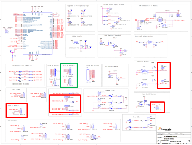
Considering S12ZVM PMSM/BLDC development kit as an example, jumper settings should be changed to have the PWM signals clear (with no external load or source, e.g. pull-ups).
| Jumper | Default settings | Configuration for the test | Notes |
| J9 | Enabled | Disabled | User On/Off switch on PT1 |
| J14 | 2-3 | Removed | EVDD / Fault input on PP0 |
| J15 | 2-3 | Removed | HALL_A / Res_A on PT1 |
| J16 | 2-3 | Removed | HALL_B / Res_B on PT2 |
| J19 | Enabled | Disabled | "Up" button on PP1 |
| J20 | Enabled | Disabled | "Down" button on PP2 |
Testing Points
Oscilloscope of sufficient parameters should be used (at least 500Ms/s) with standard low-capacitance probes or better, with isolated differential probes. Channel connection for the test should be as follows:
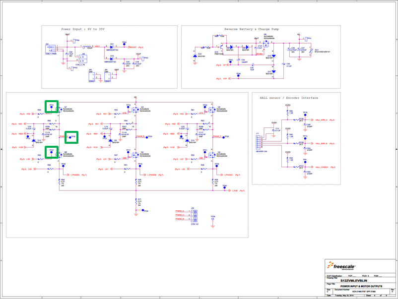
- Channel 1: PWM1_n signal to GND (for PWM1_0, PP0 on J21:1 can be used)
- Channel 2: GDU HGm or LGm signal to GND (for HG0, TP31 is used) or HGm to PHASE_m if differential probe is used (for HG0, TP31 and PHASE_A / TP35)
- Channel 3: Phase voltage on PHASE_m to GND (e.g. PHASE_A)
Software
Demo software provided on the S12ZVM PMSM/BLDC development kit page can be used for the test with minor changes:
- In "main.c", buttons and switch handling should be disabled (commented out)
INTERRUPT void ADC1done_ISR(void)
{
	static tBool getFcnStatus;

	EnableInterrupts;
	//PTT_PTT0 = 1;  // Set debug pin to record execution time
	// Read the user control interface
	//cntrState.usrControl.btSpeedUp   = PTP_PTP1;
	//cntrState.usrControl.btSpeedDown = PTP_PTP2;

	// User switch should be checked only if not in init state (see state machine table)
	//if(cntrState.state != init)
	//	cntrState.usrControl.btFlipFlop  = PTT_PTT1;

	 // User accessible switch for stopping the application.
	if (cntrState.usrControl.btFlipFlop ^ cntrState.usrControl.btFlipFlopTemp)
	{
		cntrState.usrControl.btFlipFlopTemp  = cntrState.usrControl.btFlipFlop;
		cntrState.usrControl.switchAppOnOff  = (cntrState.usrControl.btFlipFlop) ? false: true;
	}
...- In "src\S12ZVM_system\peripherals\pim.c", pin configuration should be changed as follows:
void pim_init(void)
{
  MODRR0_SCI1RR = 1; // SCI - FreeMASTER

  //DDRS_DDRS4 = 1;	// Debugg Signal
  //DDRS_DDRS5 = 1;	// Debugg Signal

  //DDRT_DDRT0 = 1;	// Debugg Signal

  MODRR1_PWMPRR = 0x01;	//PWM to pins enabled
  //DDRT_DDRT1 = 0;	// Input switch signal

}- Finally, GDU slew rate should be set to the values assumed by the application:
	  GDUSRC_GSRCHS = 7;    // High-side slew rate
	  GDUSRC_GSRCLS = 7;    // Low-side slew rate
Results
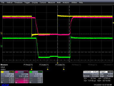
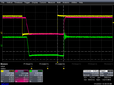
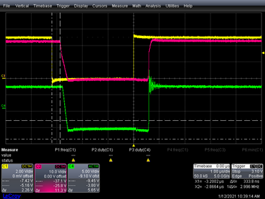
Resulting waveforms can be seen on the following figures for normal (room) conditions and using following setup:
| Item | Details |
| Oscilloscope | Lecroy WaveRunner 44Xi-A |
| Probes | PP008 / 500MHz, 10MΩ, 9.5pF |
| Evaluated PWM signal | PWM1_0 / HG0 |
|
EVB |
S12ZVMLEVBLIN Rev.D |
Two corner cases have been used to match the specifications in the Reference Manual. However, user-specific slew rate settings may be used to measure the delay in the application.
Slowest Slew Rate Settings (GDUsrc=0)
Switch-on delay:
Switch-off delay:
Fastest Slew Rate Settings (GDUsrc=0x77)
Switch-on delay:
Switch-off delay:
Summary
Measured values are compared with the Reference Manual specifications. Switch-on and switch-off delays are presented. As seen below, the results are within the specified range.
| Slew rate | Edge | Minimum | Maximum | Measured |
| Fastest slew | T_delay_ON | 0.47 μs | 0.89 μs | 0.55 μs |
| T_delay_OFF | 0.25 μs | 0.49 μs | 0.32 μs | |
| Slowest slew | T_delay_ON | 0.77 μs | 1.43 μs | 1.08 μs |
| T_delay_OFF | 0.25 μs | 0.49 μs | 0.33 μs |
For higher confidence, high temperature and low temperature tests are recommended.
Conclusion
This short article shows how to measure propagation delay between PWM signals and GDU outputs on S12ZVM using S12ZVM PMSM/BLDC development kit. The PWM to GDU propagation delay is important information for proper timing of ADC triggering if synchronized with PWM.
In simple or simplified use cases, maximum ratings of the delay can be used for consideration. However, unnecessarily higher time span between the PWM edge and ADC trigger may raise a need for lower duty-cycle limit, thus limiting the overall performance e.g. at high speed. Therefore, the importance of proper ADC triggering based on known propagation delay of PWM to GDU signal is obvious.
In addition, MOSFET turn-on and turn-off times have to be considered in the overall ADC triggering schedule, based on application-specific settings.
