- Forums
- Product Forums
- General Purpose MicrocontrollersGeneral Purpose Microcontrollers
- i.MX Forumsi.MX Forums
- QorIQ Processing PlatformsQorIQ Processing Platforms
- Identification and SecurityIdentification and Security
- Power ManagementPower Management
- MCX Microcontrollers
- S32G
- S32K
- S32V
- MPC5xxx
- Other NXP Products
- Wireless Connectivity
- S12 / MagniV Microcontrollers
- Powertrain and Electrification Analog Drivers
- Sensors
- Vybrid Processors
- Digital Signal Controllers
- 8-bit Microcontrollers
- ColdFire/68K Microcontrollers and Processors
- PowerQUICC Processors
- OSBDM and TBDML
-
- Solution Forums
- Software Forums
- MCUXpresso Software and ToolsMCUXpresso Software and Tools
- CodeWarriorCodeWarrior
- MQX Software SolutionsMQX Software Solutions
- Model-Based Design Toolbox (MBDT)Model-Based Design Toolbox (MBDT)
- FreeMASTER
- eIQ Machine Learning Software
- Embedded Software and Tools Clinic
- S32 SDK
- S32 Design Studio
- GUI Guider
- Zephyr Project
- Voice Technology
- Application Software Packs
- Secure Provisioning SDK (SPSDK)
- Processor Expert Software
- MCUXpresso Training Hub
-
- Topics
- Mobile Robotics - Drones and RoversMobile Robotics - Drones and Rovers
- NXP Training ContentNXP Training Content
- University ProgramsUniversity Programs
- Rapid IoT
- NXP Designs
- SafeAssure-Community
- OSS Security & Maintenance
- Using Our Community
-
- Cloud Lab Forums
-
- Knowledge Bases
- ARM Microcontrollers
- i.MX Processors
- Identification and Security
- Model-Based Design Toolbox (MBDT)
- QorIQ Processing Platforms
- S32 Automotive Processing Platform
- Wireless Connectivity
- CodeWarrior
- MCUXpresso Suite of Software and Tools
- MQX Software Solutions
-
- Home
- :
- QorIQ Processing Platforms
- :
- QorIQ
- :
- T2080 Refernce design IFC
T2080 Refernce design IFC
- Subscribe to RSS Feed
- Mark Topic as New
- Mark Topic as Read
- Float this Topic for Current User
- Bookmark
- Subscribe
- Mute
- Printer Friendly Page
T2080 Refernce design IFC
- Mark as New
- Bookmark
- Subscribe
- Mute
- Subscribe to RSS Feed
- Permalink
- Report Inappropriate Content
Hello Sir,
In T2080 Refernce design, I am having few queries to ask
1) what is CFG_VBANK?
2) What is the importance of CFG_VBANK in NOR flash(JS28F00AM29EWHA) 1Gb memory interface? can i remove SN74LVC1G86 IC and directly connect ifc_a7 , ifc_a6 and ifc_a5 to IFC bus?
3) what will be changes will come in the design if i want to upgrade my nor flash size?
a) to 512 megabit
b) to 2 gigabit
How many virtual bank will be require in the above mention memory sizes (512 migabit and 2gigabit)?
Waiting for your reply.
Attaching the image for your reference
Regards
Hemant
- Mark as New
- Bookmark
- Subscribe
- Mute
- Subscribe to RSS Feed
- Permalink
- Report Inappropriate Content
Hi,
One more query with respect to IFC
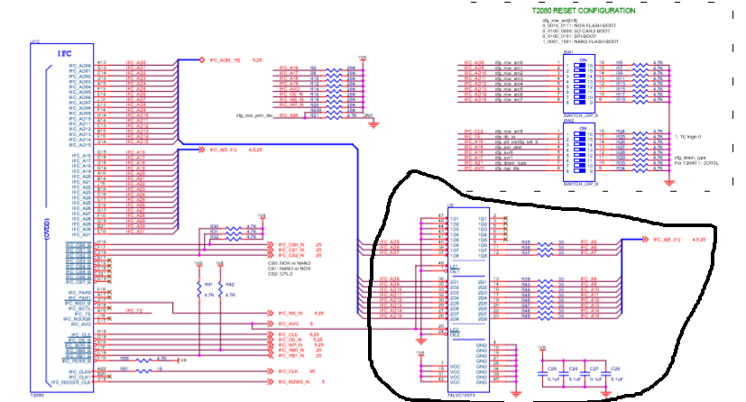
why 74LVC16373 has been used in the design? what is the importance of 74LVC16373?
attaching the image for your reference.
Regards
Hemant
- Mark as New
- Bookmark
- Subscribe
- Mute
- Subscribe to RSS Feed
- Permalink
- Report Inappropriate Content
This latch is required to provide stable Address for the NOR Flash during the read/write access from the Address/Data signals - for example refer to the QorIQ T2080 Reference Manual, Figure 13-40. Normal GPCM program operation - non-burst mode.
- Mark as New
- Bookmark
- Subscribe
- Mute
- Subscribe to RSS Feed
- Permalink
- Report Inappropriate Content
1) It is a method to "divide" single NOR Flash device into several "virtual banks" so the processor will be able to boot from anyone of them.
2) Yes.
3) You wrote:
> How many virtual bank will be require in the above mention memory sizes?
This is up to the board/application designer.
Concerning the "virtual bank" memory size please consider:
Despite that the RDB implementation gives 8 "virtual banks", only two of them are used in Linux SDK - 0 and 4.
Effectively in this case the NOR Flash is divided into two halves.
