- Forums
- Product Forums
- General Purpose MicrocontrollersGeneral Purpose Microcontrollers
- i.MX Forumsi.MX Forums
- QorIQ Processing PlatformsQorIQ Processing Platforms
- Identification and SecurityIdentification and Security
- Power ManagementPower Management
- Wireless ConnectivityWireless Connectivity
- RFID / NFCRFID / NFC
- Advanced AnalogAdvanced Analog
- MCX Microcontrollers
- S32G
- S32K
- S32V
- MPC5xxx
- Other NXP Products
- S12 / MagniV Microcontrollers
- Powertrain and Electrification Analog Drivers
- Sensors
- Vybrid Processors
- Digital Signal Controllers
- 8-bit Microcontrollers
- ColdFire/68K Microcontrollers and Processors
- PowerQUICC Processors
- OSBDM and TBDML
- S32M
- S32Z/E
-
- Solution Forums
- Software Forums
- MCUXpresso Software and ToolsMCUXpresso Software and Tools
- CodeWarriorCodeWarrior
- MQX Software SolutionsMQX Software Solutions
- Model-Based Design Toolbox (MBDT)Model-Based Design Toolbox (MBDT)
- FreeMASTER
- eIQ Machine Learning Software
- Embedded Software and Tools Clinic
- S32 SDK
- S32 Design Studio
- GUI Guider
- Zephyr Project
- Voice Technology
- Application Software Packs
- Secure Provisioning SDK (SPSDK)
- Processor Expert Software
- Generative AI & LLMs
-
- Topics
- Mobile Robotics - Drones and RoversMobile Robotics - Drones and Rovers
- NXP Training ContentNXP Training Content
- University ProgramsUniversity Programs
- Rapid IoT
- NXP Designs
- SafeAssure-Community
- OSS Security & Maintenance
- Using Our Community
-
- Cloud Lab Forums
-
- Knowledge Bases
- ARM Microcontrollers
- i.MX Processors
- Identification and Security
- Model-Based Design Toolbox (MBDT)
- QorIQ Processing Platforms
- S32 Automotive Processing Platform
- Wireless Connectivity
- CodeWarrior
- MCUXpresso Suite of Software and Tools
- MQX Software Solutions
- RFID / NFC
- Advanced Analog
-
- NXP Tech Blogs
- Home
- :
- モデルベース・デザイン・ツールボックス(MBDT)
- :
- MBDT DIYプロジェクト
- :
- OpenSDA Circuit Design & Implementation
OpenSDA Circuit Design & Implementation
- RSS フィードを購読する
- トピックを新着としてマーク
- トピックを既読としてマーク
- このトピックを現在のユーザーにフロートします
- ブックマーク
- 購読
- ミュート
- 印刷用ページ
OpenSDA Circuit Design & Implementation
- 新着としてマーク
- ブックマーク
- 購読
- ミュート
- RSS フィードを購読する
- ハイライト
- 印刷
- 不適切なコンテンツを報告
- 新着としてマーク
- ブックマーク
- 購読
- ミュート
- RSS フィードを購読する
- ハイライト
- 印刷
- 不適切なコンテンツを報告
OpenSDA is a serial and debug adapter that is built into the entire Freedom board lineup, and can also be found on other embedded boards. It provides a bridge between your computer (or other USB host) and the embedded target processor.
- 新着としてマーク
- ブックマーク
- 購読
- ミュート
- RSS フィードを購読する
- ハイライト
- 印刷
- 不適切なコンテンツを報告
Hello loverdeg@embeddedplanet.com,
Unfortunately we are not responsible with the PCB design for the EVB and the same reverse engineer we do whenever there's an issue or so.
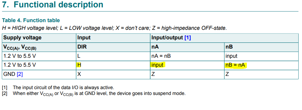
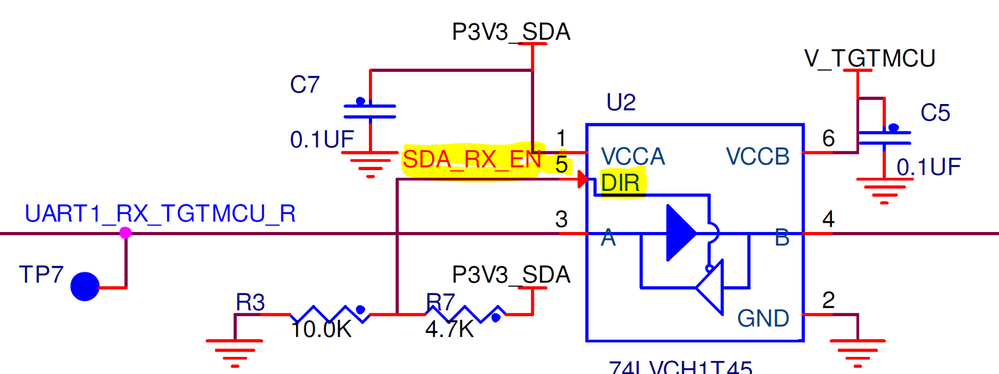
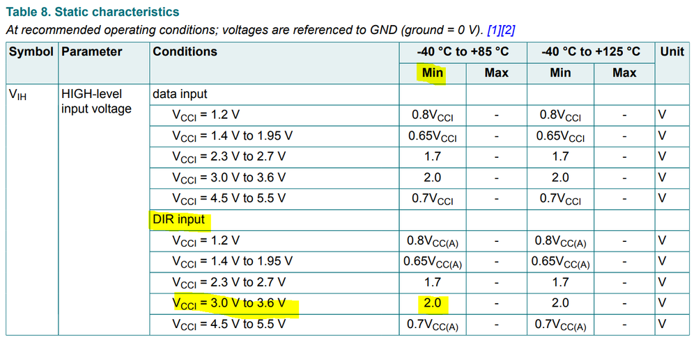
However, we do believe that the signal SDA_RX_EN might be propagated from an older, different schematic or so, which had a direction control. As you said, that looks like a voltage divider to keep the DIR up at 3V3 from 5V. Maybe this was kept or forgotten, lately connected to the 3V3 and just works due to the low 2V high logic limit of the transceiver. But it is useless to control the pin direction for the serial RX or TX because it will work in only one way. In your schematic (If you will build a PCB), I think it is safer to connect the DIR directly to the 3V3 or through a pull up resistor.
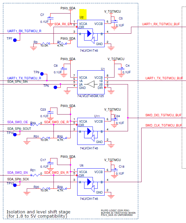
Now, for U11 and U6 the OpenSDA controls the Data and Clock direction ( Serial Wire Debugger is bidirectional communication), the same question is raised up here too: Why was the need to use a resistor level shifter from 3V3 to the 2.24V. This has the same feeling that the schematic has been propagated from another board and the level shifter was used from 5V. Same, I think it will work only with a pull up resistor from 3V3.
For the last question, I think they used for U1 a transceiver with two level shifters because for the UART_TX_MCU and the other signal the direction is always from B to A like in the Table attached. So there was no need to put two components with the DIR connected directly to ground from two signals.
The same schematic is used on the S32K EVB which strengthens my assumption that the logical design is the same on multiple boards.
If you want to design your own PCB with K22F mcu or S32K you can put just the MCU on the board, but having a header pin connected to the SWD_DIO_TGTMCU, SWD_CLK_TGTMCU and MCU's RESET pin. Keep the OpenSDA on the Eval Board and connect the EVB when programming to your board trough the J4, J10 and J13 pins. You just need to be carefull to have the same GND between the boards.
Hope this helps,
Marius
- 新着としてマーク
- ブックマーク
- 購読
- ミュート
- RSS フィードを購読する
- ハイライト
- 印刷
- 不適切なコンテンツを報告
Thanks for the assistance.
We would like to use the K20 for SWO. We know we would need to add software support for this ourselves.
Any further insight into the topic of SWO?
- 新着としてマーク
- ブックマーク
- 購読
- ミュート
- RSS フィードを購読する
- ハイライト
- 印刷
- 不適切なコンテンツを報告
Hello loverdeg@embeddedplanet.com,
In think you will find a nice tutorial here: https://mcuoneclipse.com/2016/10/17/tutorial-using-single-wire-output-swo-with-arm-cortex-m-and-ecli....
You can also have a look on this topic: https://community.nxp.com/thread/318058
Hope this helps,
Marius
- 新着としてマーク
- ブックマーク
- 購読
- ミュート
- RSS フィードを購読する
- ハイライト
- 印刷
- 不適切なコンテンツを報告
I would like to start with a question about the level-shifting logic in the OpenSDA circuit.or the OpenSDA circuit:
In viewing the schematic for the OpenSDA circuit used in the FRDM-K22F (Sheet 4, "OpenSDA Interface"), the level-shifter U2 has its direction pin (DIR, pin 5) tied between 10k/GND and 4.7k/3.3V. This brings it to about 2.24V. It is connected to a net titled SDA_RX_EN, but that net shows up nowhere else throughout the multi-page schematic, so apparently it is just a label with no external driving factor influencing it, meaning it just stays hovering at 2.24V.
The datasheet for the 74LVCH1T45 (U2) specifies that the DIR input for VCCI between 3.0V and 3.6V is a 2.0V minimum. For an application where VCCI is 3.3V, having DIR tied to 2.24V is uncomfortably close to the 2.0V edge case, especially if for no particular reason.
U2 follows a slightly different pattern than U11 and U6 since its DIR pin is being tied manually and not toggled digitally by an external pin (recall that the net it's attached to connects to nothing else in the design, even across other Freedom board designs).
So why would this pin not be tied to a solid high (P3V3_SDA) or solid low (GND)? Wouldn't residing near an edge case only be a risk for trouble? Is there something else I might be missing about this?
- 新着としてマーク
- ブックマーク
- 購読
- ミュート
- RSS フィードを購読する
- ハイライト
- 印刷
- 不適切なコンテンツを報告
Also is the reasoning for different part number on the one level shifter just to get another channel?
- 新着としてマーク
- ブックマーク
- 購読
- ミュート
- RSS フィードを購読する
- ハイライト
- 印刷
- 不適切なコンテンツを報告
adriantudor, mariuslucianandrei
Any thoughts on this ?


