- Forums
- Product Forums
- General Purpose MicrocontrollersGeneral Purpose Microcontrollers
- i.MX Forumsi.MX Forums
- QorIQ Processing PlatformsQorIQ Processing Platforms
- Identification and SecurityIdentification and Security
- Power ManagementPower Management
- Wireless ConnectivityWireless Connectivity
- RFID / NFCRFID / NFC
- Advanced AnalogAdvanced Analog
- MCX Microcontrollers
- S32G
- S32K
- S32V
- MPC5xxx
- Other NXP Products
- S12 / MagniV Microcontrollers
- Powertrain and Electrification Analog Drivers
- Sensors
- Vybrid Processors
- Digital Signal Controllers
- 8-bit Microcontrollers
- ColdFire/68K Microcontrollers and Processors
- PowerQUICC Processors
- OSBDM and TBDML
- S32M
- S32Z/E
-
- Solution Forums
- Software Forums
- MCUXpresso Software and ToolsMCUXpresso Software and Tools
- CodeWarriorCodeWarrior
- MQX Software SolutionsMQX Software Solutions
- Model-Based Design Toolbox (MBDT)Model-Based Design Toolbox (MBDT)
- FreeMASTER
- eIQ Machine Learning Software
- Embedded Software and Tools Clinic
- S32 SDK
- S32 Design Studio
- GUI Guider
- Zephyr Project
- Voice Technology
- Application Software Packs
- Secure Provisioning SDK (SPSDK)
- Processor Expert Software
- Generative AI & LLMs
-
- Topics
- Mobile Robotics - Drones and RoversMobile Robotics - Drones and Rovers
- NXP Training ContentNXP Training Content
- University ProgramsUniversity Programs
- Rapid IoT
- NXP Designs
- SafeAssure-Community
- OSS Security & Maintenance
- Using Our Community
-
- Cloud Lab Forums
-
- Knowledge Bases
- ARM Microcontrollers
- i.MX Processors
- Identification and Security
- Model-Based Design Toolbox (MBDT)
- QorIQ Processing Platforms
- S32 Automotive Processing Platform
- Wireless Connectivity
- CodeWarrior
- MCUXpresso Suite of Software and Tools
- MQX Software Solutions
- RFID / NFC
- Advanced Analog
-
- NXP Tech Blogs
Hello,
What is the recommended method to manually control the chip select when using the SPI bus? There doesn't appear to be an option to disable chip select control.
Thanks
已解决! 转到解答。
Hi,
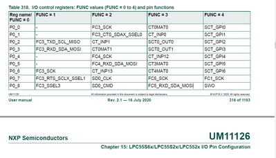
As the following SPI pins assignment, when you use FC3 as SPI master,
P0_7 FC3_RTS_SCLX_SSEL1
P0_8 FC3_SSEL3
When you configure the SPI3 control register to use the SSEL1, when you write data to SPI FIFOWR register, the FC3_RTS_SCLX_SSEL1 pin is driven to low by the spi module automatically, when the transfer is over, the pin will be driven to high automatically.
Of course, if you want to set/clear the FC3_RTS_SCLX_SSEL1 manually, as you know that the FC3_RTS_SCLX_SSEL1 is multiplexed with P0_7 pin, you can configure the P0_7 pin as GPIO, and configure it as GPIO output mode, before you write the FIFOWR register, clear the P0_7 pin by writting the GPIO output data register, after the transfer is over(you can use polling mode or interrupt mode to check the status register), you can set the P0_7 pin.
Hope it can help you
BR
XiangJun Rong
