- Forums
- Product Forums
- General Purpose MicrocontrollersGeneral Purpose Microcontrollers
- i.MX Forumsi.MX Forums
- QorIQ Processing PlatformsQorIQ Processing Platforms
- Identification and SecurityIdentification and Security
- Power ManagementPower Management
- Wireless ConnectivityWireless Connectivity
- RFID / NFCRFID / NFC
- Advanced AnalogAdvanced Analog
- MCX Microcontrollers
- S32G
- S32K
- S32V
- MPC5xxx
- Other NXP Products
- S12 / MagniV Microcontrollers
- Powertrain and Electrification Analog Drivers
- Sensors
- Vybrid Processors
- Digital Signal Controllers
- 8-bit Microcontrollers
- ColdFire/68K Microcontrollers and Processors
- PowerQUICC Processors
- OSBDM and TBDML
- S32M
- S32Z/E
-
- Solution Forums
- Software Forums
- MCUXpresso Software and ToolsMCUXpresso Software and Tools
- CodeWarriorCodeWarrior
- MQX Software SolutionsMQX Software Solutions
- Model-Based Design Toolbox (MBDT)Model-Based Design Toolbox (MBDT)
- FreeMASTER
- eIQ Machine Learning Software
- Embedded Software and Tools Clinic
- S32 SDK
- S32 Design Studio
- GUI Guider
- Zephyr Project
- Voice Technology
- Application Software Packs
- Secure Provisioning SDK (SPSDK)
- Processor Expert Software
- Generative AI & LLMs
-
- Topics
- Mobile Robotics - Drones and RoversMobile Robotics - Drones and Rovers
- NXP Training ContentNXP Training Content
- University ProgramsUniversity Programs
- Rapid IoT
- NXP Designs
- SafeAssure-Community
- OSS Security & Maintenance
- Using Our Community
-
- Cloud Lab Forums
-
- Knowledge Bases
- ARM Microcontrollers
- i.MX Processors
- Identification and Security
- Model-Based Design Toolbox (MBDT)
- QorIQ Processing Platforms
- S32 Automotive Processing Platform
- Wireless Connectivity
- CodeWarrior
- MCUXpresso Suite of Software and Tools
- MQX Software Solutions
- RFID / NFC
- Advanced Analog
-
- NXP Tech Blogs
- Home
- :
- 汎用マイクロコントローラ
- :
- LPCマイクロコントローラ
- :
- Re: LPC54616 EMC Static Memory - Burst Operation
LPC54616 EMC Static Memory - Burst Operation
- RSS フィードを購読する
- トピックを新着としてマーク
- トピックを既読としてマーク
- このトピックを現在のユーザーにフロートします
- ブックマーク
- 購読
- ミュート
- 印刷用ページ
LPC54616 EMC Static Memory - Burst Operation
- 新着としてマーク
- ブックマーク
- 購読
- ミュート
- RSS フィードを購読する
- ハイライト
- 印刷
- 不適切なコンテンツを報告
We are using the LPC54616 with an SRAM device and an FPGA on the memory bus.
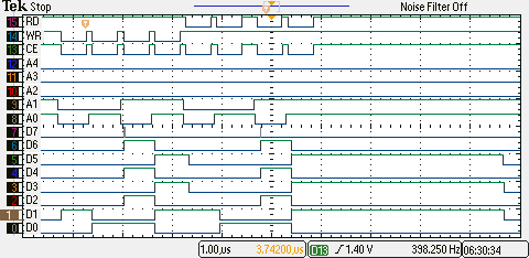
The EMC is being operated with burst mode disabled, so would expect multi-byte access to the external memory to be performed on individual read/write operation. This appears to be the case for write accesses, but not for reading, see image below...
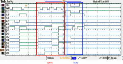
Single byte reads/writes operate as expected. All accesses to the FPGA are with single byte accesses.
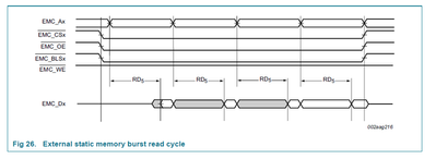
The datasheet (LPC546XX Rev 2.6) shows an example of a burst read cycle, which is what we are seeing. No example is provided for multi-byte access in non-burst mode.
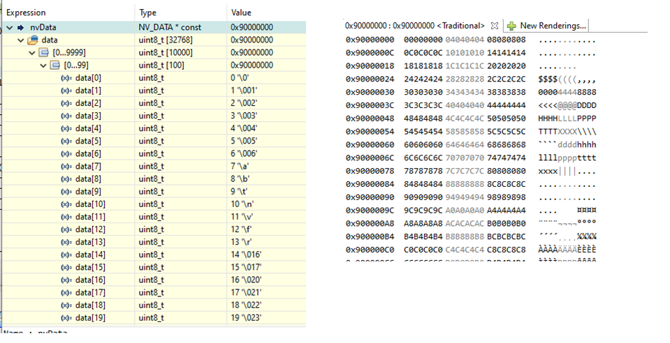
Using MCUxpresso, examining the same external memory in the Expression and Memory windows gives different results. The representations below are of the same base memory location at the same moment in time. It is assumed that the Expression window (Left-hand image) is extracting each byte individually whereas the Memory window (Right-hand image) is reading four bytes at a time.
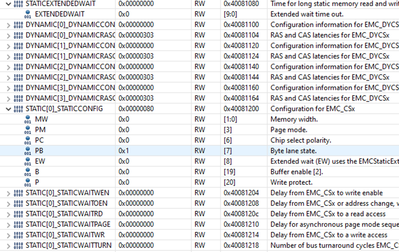
The controller registers shown below are following configuration of the EMC peripheral
- Bus Width (MW) = 8 bits
- Page Mode (PM) = Disabled
- Burst Control (EMCBC) = Disabled
- Buffer (B) = Disabled
Are there any further configuration parameters that need to be set?
Could anyone confirm/clarify the operation of the EMC with the burst mode enabled and disabled?
There are threads on a similar/same topic, but none have concluded with a suitable solution or definitive answer.
https://community.nxp.com/t5/LPC-Microcontrollers/LPC1817-EMC-Interface-read-cycle/m-p/986042
https://community.nxp.com/t5/LPC-Microcontrollers/LPC4357-bad-EMC-read-access/m-p/828257
Thanks in advance for any assistance...
- 新着としてマーク
- ブックマーク
- 購読
- ミュート
- RSS フィードを購読する
- ハイライト
- 印刷
- 不適切なコンテンツを報告
Hi,Shauno;
I think you have disabled the static memory burst mode with the STATICCONFIG0[PM]=0, with the current reading/writing, do you have any issue? for example reading data is wrong. I suppose that the reading data are okay.
For the timing circled with blur frame, the A0 address toggles at the early stage, I think the data is latched to the MCU at the rising edge of Rd or CS, the toggling A0 does not take effect on the data latch.
I suppose that you can set the delay register for example
EMCStaticWaitRd0=10;
EMCStaticWaitOen0=3;
EMCStaticWaitWr0=10;
EMCStaticWaitOen0=3;
Pls have a try.
BR
XiangJun Rong
- 新着としてマーク
- ブックマーク
- 購読
- ミュート
- RSS フィードを購読する
- ハイライト
- 印刷
- 不適切なコンテンツを報告
Thanks very much for the reply @xiangjun_rong
Setting/clearing the STATICCONFIG0[PM] bit had no effect on the reading of data. In both cases, see below, the read operation failed.
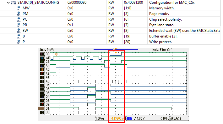
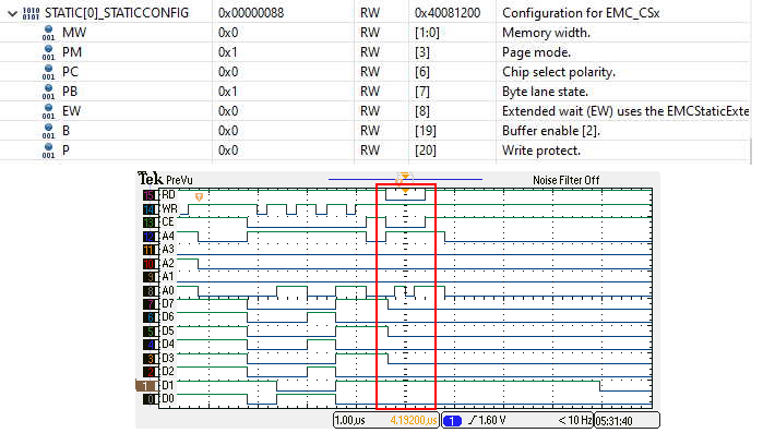
Adjusting the delay registers (EMCStaticWaitRd, EMCStaticWaitOen, EMCStaticWaitWr, EMCStaticWaitOen) again did not affect the outcome, the read operation failed.
- Writing single byte is Ok
- Reading single byte is Ok
- Writing multi-byte is Ok
- Reading multi-byte fails.
Below is example test code (note does not represent earlier waveforms) – with results in the comments
// Clear first four byte of base external NVRAM
uint8_t* ptrBase = (uint8_t*)0x90000000;
*ptrBase++ = 0;
*ptrBase++ = 0;
*ptrBase++ = 0;
*ptrBase++ = 0;

// Set test variables
uint8_t temp1 = 0;
uint16_t temp2 = 0;
uint32_t temp3 = 0;
// Set up different width pointers to base memory
uint8_t* ptr8bit = (uint8_t*)0x90000000;
uint16_t* ptr16bit = (uint16_t*)0x90000000;
uint32_t* ptr32bit = (uint32_t*)0x90000000;

// Write/Read 8-bit        // Result
*ptr8bit = 0x55;           // OK
temp1 = *ptr8bit;          // OK : temp1 = 0x55
                           // 0x90000000 = 0x55
                           // 0x90000001 = 0x00
                           // 0x90000002 = 0x00
                           // 0x90000003 = 0x00

// Write/Read 16-bit       // Result
*ptr16bit = 0xAA55;        // OK
temp2 = *ptr16bit;         // NOT OK : temp2 = 0x5555
                           // 0x90000000 = 0x55
                           // 0x90000001 = 0xAA
                           // 0x90000002 = 0x00
                           // 0x90000003 = 0x00

// Write/Read 32-bit       // Result
*ptr32bit = 0x01234567;    // OK
temp3 = *ptr32bit;         // NOT OK : temp3 = 0x67676767
                           // 0x90000000 = 0x67
                           // 0x90000001 = 0x45
                           // 0x90000002 = 0x23
                           // 0x90000003 = 0x01
The SRAM device being used latches the address on the later falling edge of either of the CE/WR or CE/RD signals depending on the operation being performed. At the moment for reading there is only a single read cycle (CE/RD) being generated for multi-byte access.
If it is not possible to configure the micro to generate read signals equivalent to how the write operation is currently performed, then the only way forward would be to modify the software to perform accesses to multi-byte SRAM variables a byte at a time.
Reading the documentation (User Manual and Datasheet), particular Section 33.10 of the User Manual seems to indicate that running the micro with burst disabled would be the solution, but it appears not to have any effect.
Thanks again in advance for any help provided.
- 新着としてマーク
- ブックマーク
- 購読
- ミュート
- RSS フィードを購読する
- ハイライト
- 印刷
- 不適切なコンテンツを報告
Hi,
It appear this is a software issue, because only 16 bits reading and 32 bits reading are not okay.
Pls try to use the code:
// Write/Read 16-bit       // Result
*ptr16bit = 0xAA55;        // OK
temp2 = (uint16_t)*ptr16bit;         // NOT OK : temp2 = 0x5555
                           // 0x90000000 = 0x55
                           // 0x90000001 = 0xAA
                           // 0x90000002 = 0x00
                           // 0x90000003 = 0x00

// Write/Read 32-bit       // Result
*ptr32bit = 0x01234567;    // OK
temp3 = (uint32_t)*ptr32bit;         // NOT OK : temp3 = 0x67676767
Pls have a try
BR
XiangJun Rong
- 新着としてマーク
- ブックマーク
- 購読
- ミュート
- RSS フィードを購読する
- ハイライト
- 印刷
- 不適切なコンテンツを報告
Thanks for the reply @xiangjun_rong.
The suggested change (explicitly casting a 32-bit value to a 32-bit value and a 16-bit value to a 16-bit value) had no effect on the operation of the read/write cycles.
There were 2 write (WR) cycles for the 16-bit access, and 4 four write (WR) cycles for the 32-bit access. In both cases for reading there was a single read (RD) cycle, with the address bus changing during the read cycle.
Do you have any example waveforms (along with example code) showing the difference in operation of the EMC with burst mode enabled and with it disabled. Or any examples showing a multi-byte read operation being performed over multiple read (RD) cycles. It may be that the micro cannot be configured this way
At the moment it appears the micro is relying solely on the data bus being updated in response to a change on the address bus, whereas the SRAM device is latching the address on a falling edge of CE/RD.
Below is an example of our previous controller (ST10) performing a similar test (i.e. writing/reading a 32-bit value). As you can see for the read operation both the CE and RD lines are being activated multiple times during the read. Is this achievable on the LPC54616?
Thanks in advance
- 新着としてマーク
- ブックマーク
- 購読
- ミュート
- RSS フィードを購読する
- ハイライト
- 印刷
- 不適切なコンテンツを報告
Hi,Shauno,
There is timing of burst reading in data sheet of LPC546xx, I attach the data sheet of LPC546xx, pls check 11.5 External memory interface.
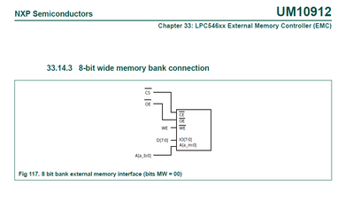
BTW, do you use Byte SRAM and connect the Byte SRAM like the following pic?
BTW, if you locate a Byte array in the external SRAM, write the array, then read the array, does the reading/writing match?
BR
XiangJun Rong
- 新着としてマーク
- ブックマーク
- 購読
- ミュート
- RSS フィードを購読する
- ハイライト
- 印刷
- 不適切なコンテンツを報告
Hi @xiangjun_rong, thanks for the reply
There is timing of burst reading in data sheet of LPC546xx, I attach the data sheet of LPC546xx, pls check 11.5 External memory interface.
Yes I've checked this burst reading waveform (see my original message). Is there a corresponding waveform example with burst read disabled?
BTW, do you use Byte SRAM and connect the Byte SRAM like the following pic?
Yes the data bus is 8-bits wide, and the signal connections are as in the diagram 33.14.3 8-bit wide memory bank connection that is shown.
BTW, if you locate a Byte array in the external SRAM, write the array, then read the array, does the reading/writing match?
Yes reading/writing a single byte as does an array of bytes works correctly.
It appears that the LPC54616 EMC peripheral only generates a single CE/RD cycle for multi-byte reads and is relying on the SRAM device to update the data bus in response to a change on the address bus.
The issue is that the SRAM device being used latches the address on the CE/RD signals going low.
Do you know if it is possible to configure the EMC peripheral to drive the read control signals in the same way as shown below (this is taken from an ST10 processor accessing the same SRAM device).
Thanks in advance
