
- Forums
- Product Forums
- General Purpose MicrocontrollersGeneral Purpose Microcontrollers
- i.MX Forumsi.MX Forums
- QorIQ Processing PlatformsQorIQ Processing Platforms
- Identification and SecurityIdentification and Security
- Power ManagementPower Management
- Wireless ConnectivityWireless Connectivity
- RFID / NFCRFID / NFC
- Advanced AnalogAdvanced Analog
- MCX Microcontrollers
- S32G
- S32K
- S32V
- MPC5xxx
- Other NXP Products
- S12 / MagniV Microcontrollers
- Powertrain and Electrification Analog Drivers
- Sensors
- Vybrid Processors
- Digital Signal Controllers
- 8-bit Microcontrollers
- ColdFire/68K Microcontrollers and Processors
- PowerQUICC Processors
- OSBDM and TBDML
- S32M
- S32Z/E
-
- Solution Forums
- Software Forums
- MCUXpresso Software and ToolsMCUXpresso Software and Tools
- CodeWarriorCodeWarrior
- MQX Software SolutionsMQX Software Solutions
- Model-Based Design Toolbox (MBDT)Model-Based Design Toolbox (MBDT)
- FreeMASTER
- eIQ Machine Learning Software
- Embedded Software and Tools Clinic
- S32 SDK
- S32 Design Studio
- GUI Guider
- Zephyr Project
- Voice Technology
- Application Software Packs
- Secure Provisioning SDK (SPSDK)
- Processor Expert Software
- Generative AI & LLMs
-
- Topics
- Mobile Robotics - Drones and RoversMobile Robotics - Drones and Rovers
- NXP Training ContentNXP Training Content
- University ProgramsUniversity Programs
- Rapid IoT
- NXP Designs
- SafeAssure-Community
- OSS Security & Maintenance
- Using Our Community
-
- Cloud Lab Forums
-
- Knowledge Bases
- ARM Microcontrollers
- i.MX Processors
- Identification and Security
- Model-Based Design Toolbox (MBDT)
- QorIQ Processing Platforms
- S32 Automotive Processing Platform
- Wireless Connectivity
- CodeWarrior
- MCUXpresso Suite of Software and Tools
- MQX Software Solutions
- RFID / NFC
- Advanced Analog
-
- NXP Tech Blogs
- Home
- :
- 汎用マイクロコントローラ
- :
- LPCマイクロコントローラ
- :
- Re: LPC4357 EMC long-long rare fail
LPC4357 EMC long-long rare fail
- RSS フィードを購読する
- トピックを新着としてマーク
- トピックを既読としてマーク
- このトピックを現在のユーザーにフロートします
- ブックマーク
- 購読
- ミュート
- 印刷用ページ
LPC4357 EMC long-long rare fail
- 新着としてマーク
- ブックマーク
- 購読
- ミュート
- RSS フィードを購読する
- ハイライト
- 印刷
- 不適切なコンテンツを報告
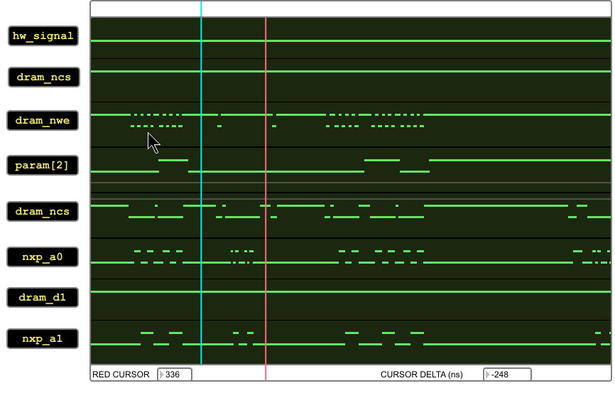
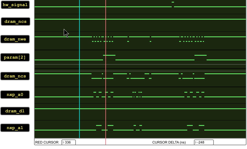
I am using the LPC3457 208 PQFP device on a custom board. I have written a lot of working firmware for it, but recently found a rare failure mode that I was able to trace back to the processor issuing a bad long long (64 bit) write cycle on the EMC bus. Traces are shown below--on the good access trace, you can see two long long writes which the processor automatically breaks into two 32bit accesses. In between are several diagnostic marker accesses (removing the diagnostic stuff has no effect on the failure mode). In the bad access trace, which happens at the same address but only occurs after about 10000 test iterations, the second long-long write occurs, but is preceded by a bogus bad 32 bit write to the same address. Here is the code that the emulator aborts on, note that the hw_signal trigger is off-screen to the right on the bad access trace.
// here is the first long long write
   *(long long *)FPGA_CHAN_DATA_H = data1;    // This is sent on second burst cycle
   wait_short(2);
         *FPGA_MODE = 0x4;     // swap longs, reset param cnt
// detect if first write fails
         if ((*FPGA_NXP_TEST & 0xffffffff00000000) == 0)
         {
            param_cnt = *FPGA_MODE;
            hw_signal();
         }
         *FPGA_MODE = 4;     // swap longs back
   wait_short(2);
// hw_signal();        Uncomment this to show the good trace
   *FPGA_MODE = 0x8;     // swap longs, reset param cnt

// here is the second long long write, it generates a bogus access about once
// every 10000 iterations.

   *(long long *)FPGA_CHAN_DATA_H = data2;    // This is sent on second burst cycle
   wait_short(10);
            param_cnt = *FPGA_MODE;
// detect if bad write occurs
         if ((*FPGA_NXP_TEST & 0xffffffff00000000) == 0)
         {
            hw_signal();
            hw_signal();
            hw_signal();
         }

Has anyone seen problems with EMC long-long accesses like this?
- 新着としてマーク
- ブックマーク
- 購読
- ミュート
- RSS フィードを購読する
- ハイライト
- 印刷
- 不適切なコンテンツを報告
Dear Robert,
You mention that the error is present at 10000 more or less, there is an specific memory region where this module fail or this is a random location every time?
Let me know your findings.
Best Regards,
Alexis Andalon
- 新着としてマーク
- ブックマーク
- 購読
- ミュート
- RSS フィードを購読する
- ハイライト
- 印刷
- 不適切なコンテンツを報告
Hi Alexis,
One more important data point I forgot to mention--the long-long data
writes and reads are aligned, address bits 2:0 are always zero for the
transfer. I do see the low addresses change as expected while the transfer
is taking place. The bogus 32-bit write goes to the same address as the
first half of the actual 64-bit write.
Robert
On Wed, Sep 18, 2019 at 8:22 PM Robert Morrison <morrisonpiano@gmail.com>
- 新着としてマーク
- ブックマーク
- 購読
- ミュート
- RSS フィードを購読する
- ハイライト
- 印刷
- 不適切なコンテンツを報告
Can't think of a systematic issue in the chip design, must be a rare race condition in my opinion.
Are you shure that
LPC_EMC->STATICCONFIG0 = 0x00000088;
is the right setting for the 8-bit wide FPGA access? The two bits which are set here
PM Page mode.
In page mode the EMC can burst up to four external accesses. Therefore devices with asynchronous page mode burst four or higher devices are supported. Asynchronous page mode burst two devices are not supported and must be accessed normally.
0 Disabled (POR reset value).
1 Async page mode enabled (page length four).
PB Byte lane state
The byte lane state bit, PB, enables different types of memory to be connected. For byte-wide static memories the BLSn[3:0] signal from the EMC is usually connected to WE (write enable). In this case for reads all the BLSn[3:0] bits must be HIGH. This means that the byte lane state (PB) bit must be LOW.
16 bit wide static memory devices usually have the BLSn[3:0] signals connected to the UBn and LBn (upper byte and lower byte) signals in the static memory. In this case a write to a particular byte must assert the appropriate UBn or LBn signal LOW. For reads, all the UB and LB signals must be asserted LOW so that the bus is driven. In this case the byte lane state (PB) bit must be HIGH.
Remark: When PB is set to 0, the WE signal is undefined or 0. You must set PB to 1, to use the WE signal.
0 For reads all the bits in BLSn[3:0] are HIGH. For writes the respective active bits in BLSn[3:0] are LOW
(POR reset value).
1 For reads the respective active bits in BLSn[3:0] are LOW. For writes the respective active bits in BLSn[3:0] are LOW.
In my opinion both bits should be 0 and not 1.
Would you be able to show the assembler code for this long-long write?
Regards,
Bernhard.
- 新着としてマーク
- ブックマーク
- 購読
- ミュート
- RSS フィードを購読する
- ハイライト
- 印刷
- 不適切なコンテンツを報告
Hi Alexis,
I've gotten quite a bit more data on the failure now,--at this point it
does look like the processor is definitely having problems doing long-long
writes (and possibly reads as well). The address is fixed at 0x1c000xxx,
this is in a bank of 1024 adresses used as a portal into an FPGA. I did
discover a pretty easy (if quite a bit slower) workaround--issuing two long
accesses in sequence with correctly shifted data never causes the failure,
I never see any extra writes with bad data.
The fail frequency is extremely variable even with no change to the
code--note for this test, no interrupts are enabled which should rule out
any interruptions to the test that might cause this fail. Sometimes I will
get an extra access fail after 10 iterations, sometimes it's in the
millions of iterations. The failure seems to be independent of the data
transferred. The 4 layer board power/ground planes are heavily bypassed, I
see no indication of erratic operation for around 30000 lines of code with
extensive testing of all data types. Only the long-long accesses seem to
somehow get confused.
Some more system data: the chip is operating at 200Mhz core frequency
from an external oscillator running at 25Mhz. The EMC bus talks to only
two devices, an SRAM and an FPGA, and I see no evidence of signal integrity
issues--other tests have run for hundreds of billions of iterations without
any failures. The EMC configuration is set as follows
// Speed up the FPGA reads and writes (0x1c000000)
LPC_EMC->CONTROL = 0x00000001; // turn off EMC reset
LPC_EMC->STATICCONFIG0 = 0x00000088; // set for 8 bit bus, enable
nwe, pagemode
LPC_EMC->STATICWAITRD0 = 0x00000004; // UPDATE SET TO 4
LPC_EMC->STATICWAITPAG0 = 0x00000001; // UPDATE SET TO 1
LPC_EMC->STATICWAITWR0 = 0x00000002; // UPDATE SET TO 2
LPC_EMC->STATICWAITTURN0 = 0x00000003; // 3 cycle turnaround
Robert