- Forums
- Product Forums
- General Purpose MicrocontrollersGeneral Purpose Microcontrollers
- i.MX Forumsi.MX Forums
- QorIQ Processing PlatformsQorIQ Processing Platforms
- Identification and SecurityIdentification and Security
- Power ManagementPower Management
- Wireless ConnectivityWireless Connectivity
- RFID / NFCRFID / NFC
- Advanced AnalogAdvanced Analog
- MCX Microcontrollers
- S32G
- S32K
- S32V
- MPC5xxx
- Other NXP Products
- S12 / MagniV Microcontrollers
- Powertrain and Electrification Analog Drivers
- Sensors
- Vybrid Processors
- Digital Signal Controllers
- 8-bit Microcontrollers
- ColdFire/68K Microcontrollers and Processors
- PowerQUICC Processors
- OSBDM and TBDML
- S32M
- S32Z/E
-
- Solution Forums
- Software Forums
- MCUXpresso Software and ToolsMCUXpresso Software and Tools
- CodeWarriorCodeWarrior
- MQX Software SolutionsMQX Software Solutions
- Model-Based Design Toolbox (MBDT)Model-Based Design Toolbox (MBDT)
- FreeMASTER
- eIQ Machine Learning Software
- Embedded Software and Tools Clinic
- S32 SDK
- S32 Design Studio
- GUI Guider
- Zephyr Project
- Voice Technology
- Application Software Packs
- Secure Provisioning SDK (SPSDK)
- Processor Expert Software
- Generative AI & LLMs
-
- Topics
- Mobile Robotics - Drones and RoversMobile Robotics - Drones and Rovers
- NXP Training ContentNXP Training Content
- University ProgramsUniversity Programs
- Rapid IoT
- NXP Designs
- SafeAssure-Community
- OSS Security & Maintenance
- Using Our Community
-
- Cloud Lab Forums
-
- Knowledge Bases
- ARM Microcontrollers
- i.MX Processors
- Identification and Security
- Model-Based Design Toolbox (MBDT)
- QorIQ Processing Platforms
- S32 Automotive Processing Platform
- Wireless Connectivity
- CodeWarrior
- MCUXpresso Suite of Software and Tools
- MQX Software Solutions
- RFID / NFC
- Advanced Analog
-
- NXP Tech Blogs
- Home
- :
- General Purpose Microcontrollers
- :
- Kinetis Microcontrollers
- :
- KL26 flash memory program and erase question
KL26 flash memory program and erase question
- Subscribe to RSS Feed
- Mark Topic as New
- Mark Topic as Read
- Float this Topic for Current User
- Bookmark
- Subscribe
- Mute
- Printer Friendly Page
KL26 flash memory program and erase question
- Mark as New
- Bookmark
- Subscribe
- Mute
- Subscribe to RSS Feed
- Permalink
- Report Inappropriate Content
[Q1] : KL26 Sub-Family Reference Manual page 27.4.9 Margin Read Commands
What are the difference between 'normal, 'user' and 'factory' levels?
What does the "user" and "factory" need to notice?
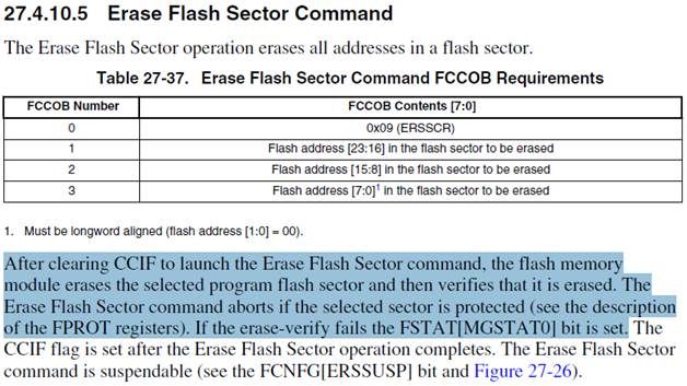
[Q2] : 27.4.10.5 Erase Flash Sector Command
if I executed the erase flash sector finished, does it will automatically execute erase_verify?
— that it is FSTAT_MGSTAT0 bit will be automatically set? if erase fail.
[Q3] : 27.4.10.1 Read 1s Section Command
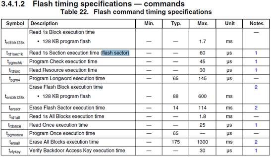
If the command can only check 4 bytes is 0xffff_ffff or not, does it execute read longword command time is same as read sector?
for example FCCOB0 = 0x01, FCCOB1-3 = 0x0_0410, FCCOB4-5 = 0x01, FCCOB6 = 0x01
[Q4] : 27.33.1 CCIF at FTFA_FSTAT
If I writing a 1 to CCIF to clear CCIF flag, can I use use while(read_CCIF == 0)() to check the CCIF flag be set or not?
Is it certain that it will be set to 1? what will happen when it execute fail?
[Q5] : 27.4.8.2 Flash commands,
Does the FCMD support erase 1 block, read 1s block command when use flash 256KB.
If what command can it need?
[Q6] : user application code in debug mode
if flash address 0x0_0000~0x0_ffff don't have boot loader code (all address is 0xFF) and when I program user application code to 0x1_000~0x1_ffff.
Does the MCU can execute the application code?
[Q7] : KDS Optimization
Can I set a void function() to specified position to a specified address? For example, in 0x0_100 – 0x0_3ff.
How I to do it?
Thanks.
- Mark as New
- Bookmark
- Subscribe
- Mute
- Subscribe to RSS Feed
- Permalink
- Report Inappropriate Content
Hello Kris,
[A1]
The user margin is a small delta to the normal read reference level and, in effect, is a minimum safety margin. If the reads pass at the tighter tolerances of the user margins, then the normal reads have at least some safety margin before users experience data loss. There are two user margin levels: user margin-1 level and user margin-0 level. User margin-1 level is the read margin to the erased state, while user margin-0 level is the read margin to the programmed state.
The following is a summary for understanding margin operation.
a) Erase Verify level is used by MCU. After erase operation MCU checks the contents using this level.
Program Verify level is same.
b) NR(Normal level) is a threshold level which decides whether flash data is "0" or "1".
If voltage value of flash cell is higher than NR, this bit is "1".
If voltage value of flash cell is lower than NR, this bit is "0".
c) Margin 0 level is for checking programming operation. (for flash data = 1).
Confirming a depth of programmed flash bit cell.
If it passed Factory Margin read 0, this means the programmed flash bit cell has
Higher voltage (more deep).
Margin 0 is same but it relates for Erase operation.
Attached to this mail, you can find a picture which indicate the level of margin.
The margin selection depends on customer requirement.
[A2]
Yes, when execute the erase flash sector finished, it will automatically execute erase_verify and if erase failed, FSTAT_MGSTAT0 bit will be automatically set.
[A3]
The Read 1s Section Command will check a section of program flash or data flash memory is erased to the specified read margin level.
The phrase size is 8 bytes, this command can check customer required numbers of phrase Flash memory size.
Such as, customer can verify 1 sector Flash size.
number = FTFx_PSECTOR_SIZE/DRD1SEC_ALIGN_SIZE;
/*! @brief P-Flash sector size */
#define FTFx_PSECTOR_SIZE 0x00000800U /* 2 KB size */
/*! @brief FlexNVM read 1s section command address alignment */
#define DRD1SEC_ALIGN_SIZE FTFx_LONGWORD_SIZE
/*! @brief Phrase size */
#define FTFx_PHRASE_SIZE 0x0008U /* 8 bytes */
[A4]
After you launch the flash operation command by writing 1 to CCIF, then you can use this code to wait the flash operation is completed:
FTFA_FSTAT = FTFA_FSTAT_CCIF_MASK;
while(!(FTFA_FSTAT & FTFA_FSTAT_CCIF_MASK));
Actually it is the same as your while(read_CCIF == 0)().
If your code is correct, the CCIF can be set after the flash command has completed.
About the flash execute fails, yes, if you enable the cpu interrupt or don't put the launch command operation in the RAM, the flash operation may be fail, can then the cpu will work unnormal, may be enter hardfault interrupt.
So, please put the flash commander launch operation function in the RAM, and disable the interrupt when you do flash operation.
[A5]
Of course the FCMD support erase block, read 1s block, it also support erase flash sector command, program longword command etc.
For details, please refer to the according reference manual, chapter FTFA, Flash command description, you will get the detail command and write sequence.
Take KL25 as an example(I don't know which kinetis chip you are using):
FCMD =0X01: Read 1s Section
FCMD =0X02:Program Check
FCMD =0X03:Read Resource
FCMD =0X06:Program Longword
FCMD =0X09:Erase Flash Sector
FCMD =0X40:Read 1s All Blocks
FCMD =0X41:Read Once
FCMD =0X43:Program Once
FCMD =0X44:Erase All Blocks
FCMD =0X45:Verify Backdoor Access Key
[A6]
Please check the below application note, this may helps
http://cache.freescale.com/files/microcontrollers/doc/user_guide/KBTLDRUG.pdf
Please let me know if this helps!
Have a great day,
Sol
-----------------------------------------------------------------------------------------------------------------------
Note: If this post answers your question, please click the Correct Answer button. Thank you!
-----------------------------------------------------------------------------------------------------------------------

