- Forums
- Product Forums
- General Purpose MicrocontrollersGeneral Purpose Microcontrollers
- i.MX Forumsi.MX Forums
- QorIQ Processing PlatformsQorIQ Processing Platforms
- Identification and SecurityIdentification and Security
- Power ManagementPower Management
- MCX Microcontrollers
- S32G
- S32K
- S32V
- MPC5xxx
- Other NXP Products
- Wireless Connectivity
- S12 / MagniV Microcontrollers
- Powertrain and Electrification Analog Drivers
- Sensors
- Vybrid Processors
- Digital Signal Controllers
- 8-bit Microcontrollers
- ColdFire/68K Microcontrollers and Processors
- PowerQUICC Processors
- OSBDM and TBDML
- S32M
-
- Solution Forums
- Software Forums
- MCUXpresso Software and ToolsMCUXpresso Software and Tools
- CodeWarriorCodeWarrior
- MQX Software SolutionsMQX Software Solutions
- Model-Based Design Toolbox (MBDT)Model-Based Design Toolbox (MBDT)
- FreeMASTER
- eIQ Machine Learning Software
- Embedded Software and Tools Clinic
- S32 SDK
- S32 Design Studio
- GUI Guider
- Zephyr Project
- Voice Technology
- Application Software Packs
- Secure Provisioning SDK (SPSDK)
- Processor Expert Software
- MCUXpresso Training Hub
-
- Topics
- Mobile Robotics - Drones and RoversMobile Robotics - Drones and Rovers
- NXP Training ContentNXP Training Content
- University ProgramsUniversity Programs
- Rapid IoT
- NXP Designs
- SafeAssure-Community
- OSS Security & Maintenance
- Using Our Community
-
- Cloud Lab Forums
-
- Knowledge Bases
- ARM Microcontrollers
- i.MX Processors
- Identification and Security
- Model-Based Design Toolbox (MBDT)
- QorIQ Processing Platforms
- S32 Automotive Processing Platform
- Wireless Connectivity
- CodeWarrior
- MCUXpresso Suite of Software and Tools
- MQX Software Solutions
-
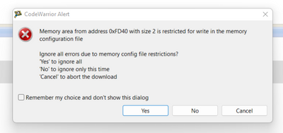
memory area from address 0xFD40 with size 2 is restricted for write in the memory configuration file
Hi NXP support team.
I using Codewarrior Version: 11.1
NMT88 EV board.
Bootloader: PE multilink
When i loading hex file i meet codeWarrior Alert " memory area from address 0xFD40 with size 2 is restricted for write in the memory configuration file"
What does this mean
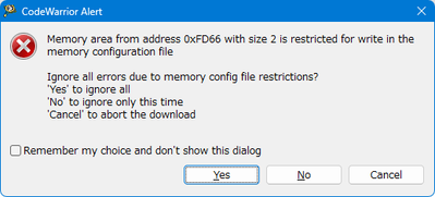
I also encountered exactly same problem with example project from NXP, "NTM88_LocAngle_XZ".
This project contains data in FLASH of address 0xFD66 - 0xFDFF, the trim area.
Can we ignore these message?
This is map file of this project.
Name                 Addr   hSize   dSize     Ref    Section   RLIB
---------------------------------------------------------------------
cau16BondwireLimits  FD66      10      16       0   .abs_section_fd66
cu16BondwireLimitXH  FD76       2       2       0   .abs_section_fd76
cu16BondwireLimitST  FD78       2       2       0   .abs_section_fd78
cu8SMISelfTestOff2   FD7E       1       1       0   .abs_section_fd7e
cu8SMISelfTestGain3  FD7F       1       1       0   .abs_section_fd7f

....

cu8Code1             FDFD       1       1       1   .abs_section_fdfd
cu8Code2             FDFE       1       1       1   .abs_section_fdfe
cu8Code3             FDFF       1       1       1   .abs_section_fdff
cu8FirmRel           FFAC       1       1       1   .abs_section_ffac
cu16TargetID         FFAD       2       2       0   .abs_section_ffad
Thanks.
Hello Windy,
I hope all is great with you.
The following response has been validated with one of our specialists:
Yes, it is normal. The warning informs the user that write and erase operations are prohibited on the trim page, in order not to erase or overwrite the trim coefficients.
So, just click “Yes” and go ahead with the programming.
In order not to see this message again, it is ok to tick “Remember my choice and don’t show this dialog”.
Please let me know if you find the information above useful.
Regards,
David
Hello Quang,
I hope all is great with you.
This is because the trim coefficients are programmed by NXP between $FD40 and $FDFF.
Writing the FLASH memory is done byte by byte, but erasing it is done page by page. In the NTM88, a page is 512-byte long and the full FLASH memory contains 16 pages. The trim coefficients are located in the page that starts at address $FC00 and ends at address $FDFF.
I do not recommend to erase such values.
I hope this information helps.
Regards,
David
Hello Quang,
I am pleased to contact you again.
In this case, I do recommend running an example project and use it as a reference for your design. It would be helpful if you reviewed the FLASH memory handling.
Please let me know if you find the information above useful.
Regards,
David
I am really sorry I did not get properly your question, can you please give me more information
also please tell us the part number that you are using
regards
Hi Vicentegomez,
Sorry for my late reply, i am in vacation of new lunar year in Vietnam.
I mean when i flash the hex file in to NTM88H055 IC,
I meet this alert " memory area from address 0xFD40 with size 2 is restricted for write in the memory configuration file"
So i worry about this alert make my code run fail.
But i check with this alert, my program run normal.
I don't know this alert for exactly what warning? Can you explain more for this alert?
thanks and best regards,

