- Forums
- Product Forums
- General Purpose MicrocontrollersGeneral Purpose Microcontrollers
- i.MX Forumsi.MX Forums
- QorIQ Processing PlatformsQorIQ Processing Platforms
- Identification and SecurityIdentification and Security
- Power ManagementPower Management
- MCX Microcontrollers
- S32G
- S32K
- S32V
- MPC5xxx
- Other NXP Products
- Wireless Connectivity
- S12 / MagniV Microcontrollers
- Powertrain and Electrification Analog Drivers
- Sensors
- Vybrid Processors
- Digital Signal Controllers
- 8-bit Microcontrollers
- ColdFire/68K Microcontrollers and Processors
- PowerQUICC Processors
- OSBDM and TBDML
- S32M
-
- Solution Forums
- Software Forums
- MCUXpresso Software and ToolsMCUXpresso Software and Tools
- CodeWarriorCodeWarrior
- MQX Software SolutionsMQX Software Solutions
- Model-Based Design Toolbox (MBDT)Model-Based Design Toolbox (MBDT)
- FreeMASTER
- eIQ Machine Learning Software
- Embedded Software and Tools Clinic
- S32 SDK
- S32 Design Studio
- GUI Guider
- Zephyr Project
- Voice Technology
- Application Software Packs
- Secure Provisioning SDK (SPSDK)
- Processor Expert Software
- MCUXpresso Training Hub
-
- Topics
- Mobile Robotics - Drones and RoversMobile Robotics - Drones and Rovers
- NXP Training ContentNXP Training Content
- University ProgramsUniversity Programs
- Rapid IoT
- NXP Designs
- SafeAssure-Community
- OSS Security & Maintenance
- Using Our Community
-
- Cloud Lab Forums
-
- Knowledge Bases
- ARM Microcontrollers
- i.MX Processors
- Identification and Security
- Model-Based Design Toolbox (MBDT)
- QorIQ Processing Platforms
- S32 Automotive Processing Platform
- Wireless Connectivity
- CodeWarrior
- MCUXpresso Suite of Software and Tools
- MQX Software Solutions
-
- Home
- :
- Product Forums
- :
- 8-bit Microcontrollers
- :
- Re: Fixed Frequency Clock for FTM S08PA60
Fixed Frequency Clock for FTM S08PA60
- Subscribe to RSS Feed
- Mark Topic as New
- Mark Topic as Read
- Float this Topic for Current User
- Bookmark
- Subscribe
- Mute
- Printer Friendly Page
Fixed Frequency Clock for FTM S08PA60
- Mark as New
- Bookmark
- Subscribe
- Mute
- Subscribe to RSS Feed
- Permalink
- Report Inappropriate Content
Hi,
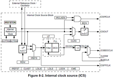
I have a big lost time during many days to understand how Fixed Frequency Clock is generated, because i need a lower frequency for my PWM application.
It's impossible to know what is exactly the frenquency clock in my FTM1 module.
Idealy, i need a FTM clock at 12.8µs.
My PA60 running fully with an external cristal oscillator at 20Mhz, so 0,05µs of period busclock (BDIV0).
If i take datasheet, i set RDIV to 128, so 0.05 * 128 = 6.4µs :
ICS_C1 = 0x90;        //div128
ICS_OSCSC_RANGE = 1;
Then, datasheet explains ICSFFCLK is divided by 2, so 6.4 * 2 = 12.8µs:
And i use a div1 in my FTM1 module with external clock selected.
If i generate a minimal PWM signal at 50% of duty, oscilloscope give me a signal arround 20µs. And it's not a multiple of busclock divided... i don't understand. !!
Anyone can explain me how can i determinate the FFCLK exactly please ?
Thank you,
Sylvain
- Mark as New
- Bookmark
- Subscribe
- Mute
- Subscribe to RSS Feed
- Permalink
- Report Inappropriate Content
Hi @Julián_AragónM , thank you repli me.
It's true, i never check ICSOUT really as output pin. I will do it. However, I'm using also RTC for real Clock system, MTIM, I2C, SPI FTM and One-wire bus, based on Fbus at 20MHz, so i can confirm there is no problem. But i will check.
Here is my ICS and FTM modules settings (sorry i write too quick, i selected "Fixed Frequency Clock in FTM, not "External Clock)
	/* Set the ICS Internal Clock System */
	/* Enable 20MHz crystal to find 20MHz bus clock */
	ICS_OSCSC = 0x96; 							/* high-range, high-gain, oscillator required */
	while (ICS_OSCSC_OSCINIT == 0); 			/* waiting until oscillator is ready */
	ICS_C1 = 0x80; 								/* external clock reference (20MHZ) to FLL output */
	ICS_C2 = 0x00; 								/* BDIV = 0, prescalar = 1 */

	/* Set the ICS Internal Clock System */
	/* Enable Fixed Frequency Clock for FTM module ICSFFCK */
	ICS_C1 = 0x90;								/* RDIV = 128 with RANGE = 1 */
	ICS_OSCSC_RANGE = 1;						/* Give 20MHz / 128 = 156.250KHz so FFCK period = 6.4µS*/
FTM1_SC = 0x11; // No IT, up counting mode, div2, div2 => div4, Fixed frequency clock => FTM ON (6.4µs * 2 * 2 = 25.6µs)
FTM1_C0SC = 0xA8; // No IT, Edge-Aligned PWM
Thank you
- Mark as New
- Bookmark
- Subscribe
- Mute
- Subscribe to RSS Feed
- Permalink
- Report Inappropriate Content
Hi @corso66,
From your code snippet, the configuration seems to be correct. Just help me checking if the FTMx_MODE is configured as Write Protected Disabled, since both CLKS and PS from FTMx_SC are write protected, and these bits can be written only if MODE[WPDIS] = 1.
Best regards,
Julián.
- Mark as New
- Bookmark
- Subscribe
- Mute
- Subscribe to RSS Feed
- Permalink
- Report Inappropriate Content
Hi @corso66,
Could you firstly confirm if your external oscillator is running at the desired frequency? Measuring it directly and the enabling bus clock output pin.
Also, please share the configuration of the FTMx_SC register, as on the Clock Source Selection field, selecting "External Clock" may select TCLK1 as the clock source for FTM1.
Best regards,
Julián.


