- NXP Forums
- Product Forums
- General Purpose MicrocontrollersGeneral Purpose Microcontrollers
- i.MX Forumsi.MX Forums
- QorIQ Processing PlatformsQorIQ Processing Platforms
- Identification and SecurityIdentification and Security
- Power ManagementPower Management
- MCX Microcontrollers
- S32G
- S32K
- S32V
- MPC5xxx
- Other NXP Products
- Wireless Connectivity
- S12 / MagniV Microcontrollers
- Powertrain and Electrification Analog Drivers
- Sensors
- Vybrid Processors
- Digital Signal Controllers
- 8-bit Microcontrollers
- ColdFire/68K Microcontrollers and Processors
- PowerQUICC Processors
- OSBDM and TBDML
-
- Solution Forums
- Software Forums
- MCUXpresso Software and ToolsMCUXpresso Software and Tools
- CodeWarriorCodeWarrior
- MQX Software SolutionsMQX Software Solutions
- Model-Based Design Toolbox (MBDT)Model-Based Design Toolbox (MBDT)
- FreeMASTER
- eIQ Machine Learning Software
- Embedded Software and Tools Clinic
- S32 SDK
- S32 Design Studio
- GUI Guider
- Zephyr Project
- Voice Technology
- Application Software Packs
- Secure Provisioning SDK (SPSDK)
- Processor Expert Software
-
- Topics
- Mobile Robotics - Drones and RoversMobile Robotics - Drones and Rovers
- NXP Training ContentNXP Training Content
- University ProgramsUniversity Programs
- Rapid IoT
- NXP Designs
- SafeAssure-Community
- OSS Security & Maintenance
- Using Our Community
-
- Cloud Lab Forums
-
- Home
- :
- General Purpose Microcontrollers
- :
- Kinetis Microcontrollers
- :
- FTM Filter for Input Capture not working
FTM Filter for Input Capture not working
- Subscribe to RSS Feed
- Mark Topic as New
- Mark Topic as Read
- Float this Topic for Current User
- Bookmark
- Subscribe
- Mute
- Printer Friendly Page
FTM Filter for Input Capture not working
- Mark as New
- Bookmark
- Subscribe
- Mute
- Subscribe to RSS Feed
- Permalink
- Report Inappropriate Content
I'm sending a 0-5 V square wave signal into FTM1_CH0 of a K64, with the input filter value set to 16, and the mode set to detect rising edges. By my understanding, that means that the FTM requires the input signal to remain in a high state for 16 bus clock cycles (i.e. 260 ns with bus clock = 60 MHz) following a low-to-high transition before it sets the CHnF flag and writes the input capture register C(n)V with the counter value. However, I've discovered that the FTM is occasionally counting small glitches on the input signal as a true edge.
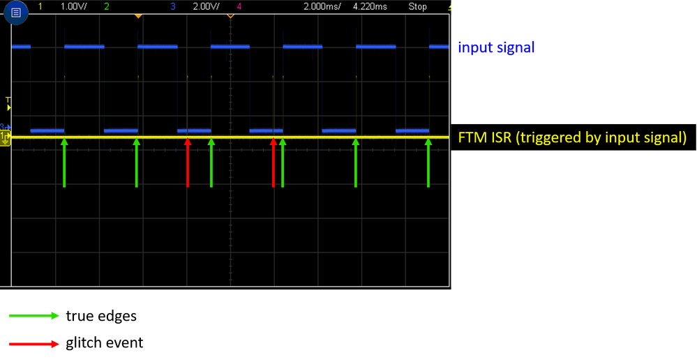
Above is a scope trace showing six true edges and two glitch events that cause false edge triggers. To capture this scope trace, I have caused a GPIO pin to toggle (channel 1, yellow) in the FTM ISR that is fired whenever an edge is detected on the input signal (channel 3, blue).
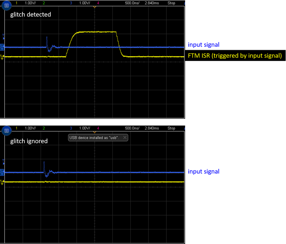
Zooming in on the glitch events, I see that they do not last the minimum duration set by the input filter value (there is a very brief spike, < 50 ns, on the input signal). Furthermore, the input high level is not > 0.7*V_DD, as required to be considered an input high voltage. (I have V_DD set to 1.8 V, so the input signal needs to be at least 1.26 V. Here it looks like it maybe reaches 800 mV... although perhaps maybe my scope is not resolving the true peak height). Lastly, you can also see that this type of glitch event does not always cause an edge detection event (bottom panel).
What would the reason be for this sort of behavior of the FTM input capture filter for edge detection?
- Mark as New
- Bookmark
- Subscribe
- Mute
- Subscribe to RSS Feed
- Permalink
- Report Inappropriate Content
Hi, Andy,
The minimum pulse cycle time is CHnFVAL[3:0] (× 4 system clocks), assume that the system clock is 120MHz for the K64, the minimum pulse cycle time is 16*[1/(120MHz/4)]=500ns.
You says that the capture signal is 5V logic, if you inputs 3.3V logic capture signal, what is the result?
BR
XiangJun Rong
- Mark as New
- Bookmark
- Subscribe
- Mute
- Subscribe to RSS Feed
- Permalink
- Report Inappropriate Content
Hi,
This hasn't answered the question.
I have a similar problem:
SystemClk = 120MHz; Pre-scaler = divide by 1
Filter:
The signal to be captured by FTM1 Ch0 is Freq_Mon = 1MHz.
The signal when present has been verified by oscilloscope.
The minimum pulse width to be passed by the filter is:
1/2 Freq_Mon = 500ns.
From the manual [Ref: P972 K24 Sub-Family Reference Manual, Rev. 2, January 2014]
it states that:
minimum pulse width = CHnFVAL[3:0] x 4 system clocks
4 system clocks = 1/120MHz x 4
= 8.3ns x 4
= 33.33ns
so
CHnFVAL[3:0] = 500ns / 33.33ns
= 15 // Stops capturing. Tried 14 and get same result
However:
Setting CHnFVAL[3:0] = 7 passes a pulse of 500ns
Setting CHnFVAL[3:0] = 8 stops a pulse of 500ns
This infers the system clock is divided by 2. i.e. 60MHz
e.g.
4 system clocks = 1/60MHz x 4
= 16.67ns x 4
= 66.67ns
so
CHnFVAL[3:0] = 500ns / 66.67ns
= 7.5 (7) works fine, but I don't understand why?
Implementation:
void FTM1_DRV_InputCaptureInit(void)
{
    // Enable clock to the FTM1 module
    SIM_SCGC6 |= SIM_SCGC6_FTM1_MASK;

    // Configure pin 64 and its alternate function for FTM1 Ch 0. pin PTA12 (64)
    PORTA_PCR12 = PORT_PCR_MUX(3);

    // Disable write protection for FTM1 registers
    FTM1_MODE |= FTM_MODE_WPDIS_MASK;

    // Configure FTM1 as input capture
    FTM1_SC = 0;                        // Ensure FTM1 is disabled for setup
    FTM1_SC &= ~FTM_SC_TOIE_MASK;       // Disable Timer Overflow Interrupt
    FTM1_SC &= ~FTM_SC_TOF_MASK;        // Clear Timer Overflow Event flag
    FTM1_CNTIN = 0;                     // Count reset to 0
    FTM1_MOD = 0xFFFF;                  // Set the modulo register for maximum count

    // The clk source is set to 120MHz by FTM1_DRV_CaptureStart() every 500ms.
    FTM1_SC &= ~FTM_SC_CLKS(7);         // Select NO clock.
    FTM1_SC |= FTM_SC_PS(0);            // Select prescaler divide by 1.

    // Configure FTM1 Channel 0 for input capture on rising edge only
    FTM1_C0SC = FTM_CnSC_ELSA_MASK;     // Capture on rising edge

    FTM1_FILTER |= FTM_FILTER_CH0FVAL(7);  // Half the input period
                                           // (120MHz / 4) x FVAL = 500ns
                                           // FVAL = 500 / 33.33 = 15.
                                           // This value stops the ISR
                                           // (Using 60MHz / 4) x FVAL = 500ns
                                           // FVAL = 500 / 66.67 = 7.5
                                           // Use 7 and runs ok
                                           // Dont know why using the value of
                                           // SYS_CLK doesnt work.
                                           // The frequency set in SC reg is SYS_CLK

#ifdef DEBUG_CPT
    // Enable CAPTEST mode for FTM1 (simulate input capture events internally)
    FTM1_CONF |= FTM_CONF_CAPTEST_MASK;
#endif

    /* Configure NVIC. Register interrupt into Ram Vector table */
    os_install_int_handler (g_ftmIrqId[HW_FTM1], FTM1_ISR);

    NVIC_SetPriority(FTM1_IRQn, 1); // ISR runs every 500ms for ?ns

    NVIC_ClearPendingIRQ(g_ftmIrqId[HW_FTM1]);

    /* Enable FTM interrupt in NVIC level.*/
    INT_SYS_EnableIRQ(g_ftmIrqId[HW_FTM1]);

    // Make sure these are reset at initailization.
    count = 0;
    freq_mon_fault = false;
}
- Mark as New
- Bookmark
- Subscribe
- Mute
- Subscribe to RSS Feed
- Permalink
- Report Inappropriate Content
I figured out the question of signal magnitude: with such a short pulse, the cable I was using to probe the CH3 signal in the above figures was loading down the input signal. By using a scope probe cable instead of a BNC cable, I could see that the signal could very well be rising to the 0.7*V_DD threshold to be considered an input high voltage level.
Nevertheless, the issue of FTM Input Filtering remains. The pulse duration is less than 16 times the FTM source clock, so I still believe that this short pulse should not be triggering the FTM.


