- Forums
- Product Forums
- General Purpose MicrocontrollersGeneral Purpose Microcontrollers
- i.MX Forumsi.MX Forums
- QorIQ Processing PlatformsQorIQ Processing Platforms
- Identification and SecurityIdentification and Security
- Power ManagementPower Management
- MCX Microcontrollers
- S32G
- S32K
- S32V
- MPC5xxx
- Other NXP Products
- Wireless Connectivity
- S12 / MagniV Microcontrollers
- Powertrain and Electrification Analog Drivers
- Sensors
- Vybrid Processors
- Digital Signal Controllers
- 8-bit Microcontrollers
- ColdFire/68K Microcontrollers and Processors
- PowerQUICC Processors
- OSBDM and TBDML
-
- Solution Forums
- Software Forums
- MCUXpresso Software and ToolsMCUXpresso Software and Tools
- CodeWarriorCodeWarrior
- MQX Software SolutionsMQX Software Solutions
- Model-Based Design Toolbox (MBDT)Model-Based Design Toolbox (MBDT)
- FreeMASTER
- eIQ Machine Learning Software
- Embedded Software and Tools Clinic
- S32 SDK
- S32 Design Studio
- GUI Guider
- Zephyr Project
- Voice Technology
- Application Software Packs
- Secure Provisioning SDK (SPSDK)
- Processor Expert Software
- MCUXpresso Training Hub
-
- Topics
- Mobile Robotics - Drones and RoversMobile Robotics - Drones and Rovers
- NXP Training ContentNXP Training Content
- University ProgramsUniversity Programs
- Rapid IoT
- NXP Designs
- SafeAssure-Community
- OSS Security & Maintenance
- Using Our Community
-
- Cloud Lab Forums
-
- Knowledge Bases
- Home
- :
- i.MX Forums
- :
- i.MX Processors
- :
- Re: i.MX6ULL RM CSI interface shifted
i.MX6ULL RM CSI interface shifted
- Subscribe to RSS Feed
- Mark Topic as New
- Mark Topic as Read
- Float this Topic for Current User
- Bookmark
- Subscribe
- Mute
- Printer Friendly Page
- Mark as New
- Bookmark
- Subscribe
- Mute
- Subscribe to RSS Feed
- Permalink
- Report Inappropriate Content
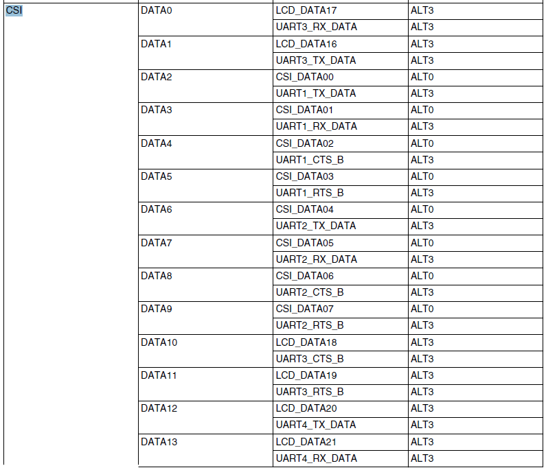
according to the i.MX6ULL reference manual (p 1666/4127 ... 1673) ALT0 for
CSI_DATA00 is CSI_DATA02
CSI_DATA01 is CSI_DATA03
...
CSI_DATA07 is CSI_DATA09
thats somehow strange, shouldn't has ALT0 the same CSI data numbering as the pad name?
Solved! Go to Solution.
- Mark as New
- Bookmark
- Subscribe
- Mute
- Subscribe to RSS Feed
- Permalink
- Report Inappropriate Content
Hi Chris,
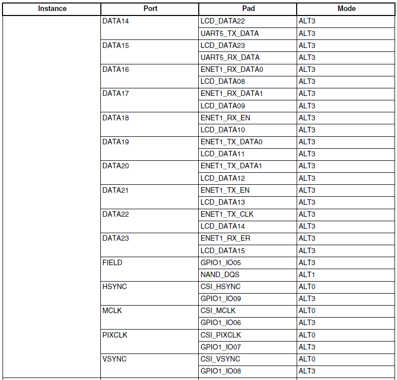
i.M6ULL has only 289 ball pads, all functional signals can not be escaped out at the same time, they will be multiplexed in different group pins instead. For CSI module, only CSI_MCLK, CSI_PICCLK, CSI_VSYNC, CSI_HSYNC and CSI_DATA[07:00] ball pads are defined and escaped out. As described in 4.1.1 Muxing Options table, the ball pads CSI_DATA[07:00] are mapped to the internal CSI module functional signals CSI_DATA[9:2].
On our EVK board, it uses only 8-bit CSI data lines (CSI_DATA[07:00] -> CSI_DATA[9:2]). When connect to an external 10-bit sensor, the least 2 bits are not used, and our SDK handles it in this way also. If customers want to use the full 10 bits or even more data bits, they can multiplex them to ball pads as 4.1.1 Muxing Options table.
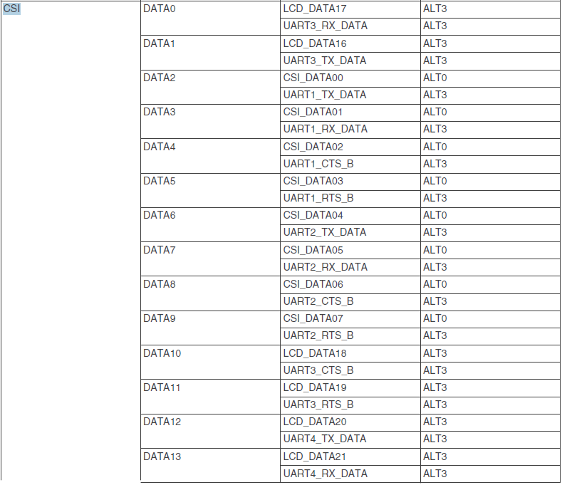
The CSI module signal CSI_DATA0 can be multiplexed on ball pad LCD_DATA17 or UART3_RX_DATAbut not on ball pad of CSI_DATA00.
It is not so good to name the net name of CSI_DATA[07_00] ball pads connection as CSI_DATA[7:0] on the EVK schematic, but there is not typo in this RM section.
Best regards,
Carlos
- Mark as New
- Bookmark
- Subscribe
- Mute
- Subscribe to RSS Feed
- Permalink
- Report Inappropriate Content
Hi chris321,
The RM description is correct. The CSI module can support 24-bit data with DATA[9:2] multiplexed to pads CSI_DATA[07:00], DATA1 multiplexed to pad LCD_DATA16 and DATA0 multiplexed to LCD_DATA17. For more detail, please refer to the 4.1.1 Muxing Options Table. Thanks!
Regards,
Carlos
NXP Technical Support
-----------------------------------------------------------------------------------------------------------------------
Note: If this post answers your question, please click the Correct Answer button. Thank you!
-----------------------------------------------------------------------------------------------------------------------
- Mark as New
- Bookmark
- Subscribe
- Mute
- Subscribe to RSS Feed
- Permalink
- Report Inappropriate Content
Hi Carlos,
According to the table you copied from the RM the signal CSI_DATA0 is available at pin LCD_DATA17 (B13) but not available on CSI_DATA00 (E4).
Correct?
- Mark as New
- Bookmark
- Subscribe
- Mute
- Subscribe to RSS Feed
- Permalink
- Report Inappropriate Content
Hi chris,
that is correct.
- Mark as New
- Bookmark
- Subscribe
- Mute
- Subscribe to RSS Feed
- Permalink
- Report Inappropriate Content
Ok thank you for your time.
But I just found that in the reference schematic SPF-29364_a the signal CSI_DATA0 is connected to pin CSI_DATA00. That conflicts somehow with the above.
- Mark as New
- Bookmark
- Subscribe
- Mute
- Subscribe to RSS Feed
- Permalink
- Report Inappropriate Content
Let me check.
- Mark as New
- Bookmark
- Subscribe
- Mute
- Subscribe to RSS Feed
- Permalink
- Report Inappropriate Content
Hi Chris,
i.M6ULL has only 289 ball pads, all functional signals can not be escaped out at the same time, they will be multiplexed in different group pins instead. For CSI module, only CSI_MCLK, CSI_PICCLK, CSI_VSYNC, CSI_HSYNC and CSI_DATA[07:00] ball pads are defined and escaped out. As described in 4.1.1 Muxing Options table, the ball pads CSI_DATA[07:00] are mapped to the internal CSI module functional signals CSI_DATA[9:2].
On our EVK board, it uses only 8-bit CSI data lines (CSI_DATA[07:00] -> CSI_DATA[9:2]). When connect to an external 10-bit sensor, the least 2 bits are not used, and our SDK handles it in this way also. If customers want to use the full 10 bits or even more data bits, they can multiplex them to ball pads as 4.1.1 Muxing Options table.
The CSI module signal CSI_DATA0 can be multiplexed on ball pad LCD_DATA17 or UART3_RX_DATAbut not on ball pad of CSI_DATA00.
It is not so good to name the net name of CSI_DATA[07_00] ball pads connection as CSI_DATA[7:0] on the EVK schematic, but there is not typo in this RM section.
Best regards,
Carlos
- Mark as New
- Bookmark
- Subscribe
- Mute
- Subscribe to RSS Feed
- Permalink
- Report Inappropriate Content
Hi Carlos,
I am aware that ALT0 doesn't has to be the main function and thus the pin name.
CSI_DATA00 function is not available on CSI_DATA00 pin according to the MUX table, that's whats confusing me.
- Mark as New
- Bookmark
- Subscribe
- Mute
- Subscribe to RSS Feed
- Permalink
- Report Inappropriate Content
Ok ok, now I goy you.
Let me check, sounds like a typo.
Thanks Carlos
- Mark as New
- Bookmark
- Subscribe
- Mute
- Subscribe to RSS Feed
- Permalink
- Report Inappropriate Content
Hi chris321,
As you may know each pin on i.MX devices has up to 8 potential functions, and on the other side, one function can be available in different pins.
One of the 8 functions is chosen as the "main" function and this is how the pin will be named, but it is not necessary to be ALT 0, it could be any.
Regards,
Carlos


