- NXP Forums
- Product Forums
- General Purpose MicrocontrollersGeneral Purpose Microcontrollers
- i.MX Forumsi.MX Forums
- QorIQ Processing PlatformsQorIQ Processing Platforms
- Identification and SecurityIdentification and Security
- Power ManagementPower Management
- MCX Microcontrollers
- S32G
- S32K
- S32V
- MPC5xxx
- Other NXP Products
- Wireless Connectivity
- S12 / MagniV Microcontrollers
- Powertrain and Electrification Analog Drivers
- Sensors
- Vybrid Processors
- Digital Signal Controllers
- 8-bit Microcontrollers
- ColdFire/68K Microcontrollers and Processors
- PowerQUICC Processors
- OSBDM and TBDML
-
- Solution Forums
- Software Forums
- MCUXpresso Software and ToolsMCUXpresso Software and Tools
- CodeWarriorCodeWarrior
- MQX Software SolutionsMQX Software Solutions
- Model-Based Design Toolbox (MBDT)Model-Based Design Toolbox (MBDT)
- FreeMASTER
- eIQ Machine Learning Software
- Embedded Software and Tools Clinic
- S32 SDK
- S32 Design Studio
- GUI Guider
- Zephyr Project
- Voice Technology
- Application Software Packs
- Secure Provisioning SDK (SPSDK)
- Processor Expert Software
-
- Topics
- Mobile Robotics - Drones and RoversMobile Robotics - Drones and Rovers
- NXP Training ContentNXP Training Content
- University ProgramsUniversity Programs
- Rapid IoT
- NXP Designs
- SafeAssure-Community
- OSS Security & Maintenance
- Using Our Community
-
- Cloud Lab Forums
-
Hi all
I have a question about Sensor Interface Timings.
Especially, Gated Clock Mode and Non-Gated Clock Mode.
Q1.
Is the data latched at the rising edge of the valid pixel clock ?
In IMX6SDLIEC Rev. 7, 10/2016 , there are following description for Sensor Interface Timing in Gated Clock Mode.
"Data is latched at the rising edge of the valid pixel clocks."
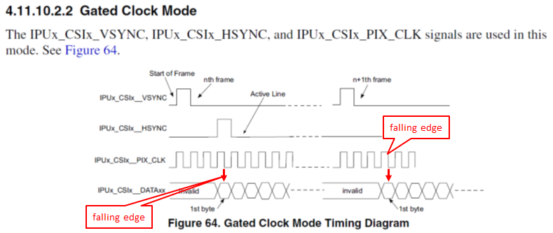
However, it looks the data is latched at falling edge in the Figure 58 of IMX6SDLIEC Rev. 7, 10/2016.
Which is correct ?
Q2.
Is the data latched at the rising edge of the valid pixel clock ?
In IMX6SDLIEC Rev. 7, 10/2016 , there are following description for Sensor Interface Timing in Non-Gated Clock Mode.
"The timing is the same as the gated-clock mode”
However, in the Figure 38-17 and Figure 38-18 of RM, the edge is the oppsite.
Is the data latched at the rising edge of the valid pixel clock in Non-Gated Clock Mode ?
Ko-hey
已解决! 转到解答。
Hi Ko-hey
yes data is latched at the rising edge of pixel clock and
this is valid for Non-Gated Clock Mode too. Please note there is
IPUx_CSI0_SENS_CONF[CSI0_SENS_PIX_CLK_POL] bit which selects the
polarity of pixel clock, described in sect.38.5.151 CSI0 Sensor Configuration Register
(IPUx_CSI0_SENS_CONF) i.MX6SDL Reference Manual
http://cache.freescale.com/files/32bit/doc/ref_manual/IMX6SDLRM.pdf
Best regards
igor
-----------------------------------------------------------------------------------------------------------------------
Note: If this post answers your question, please click the Correct Answer button. Thank you!
-----------------------------------------------------------------------------------------------------------------------
Hi Igor
Let me confirm more.
According to the Figure 64, the IPUx_CSIx_DATA is latched at falling edge of IPUx_CSIx_PIX_CLK in Gated clock mode.
However, you answered that data is latched at the rising edge of pixel clock.
So the following figure is wrong. Am I correct ?
If yes, do you have any plan to revise it ?
Ko-hey
Hi Ko-hey
data is latched at the rising edge of pixel clock.
As the polarity of pixel clock can be changed with
IPUx_CSI0_SENS_CONF[CSI0_SENS_PIX_CLK_POL]
so picture above can be consdired as correct too.
Best regards
igor
