- NXP Forums
- Product Forums
- General Purpose MicrocontrollersGeneral Purpose Microcontrollers
- i.MX Forumsi.MX Forums
- QorIQ Processing PlatformsQorIQ Processing Platforms
- Identification and SecurityIdentification and Security
- Power ManagementPower Management
- MCX Microcontrollers
- S32G
- S32K
- S32V
- MPC5xxx
- Other NXP Products
- Wireless Connectivity
- S12 / MagniV Microcontrollers
- Powertrain and Electrification Analog Drivers
- Sensors
- Vybrid Processors
- Digital Signal Controllers
- 8-bit Microcontrollers
- ColdFire/68K Microcontrollers and Processors
- PowerQUICC Processors
- OSBDM and TBDML
-
- Solution Forums
- Software Forums
- MCUXpresso Software and ToolsMCUXpresso Software and Tools
- CodeWarriorCodeWarrior
- MQX Software SolutionsMQX Software Solutions
- Model-Based Design Toolbox (MBDT)Model-Based Design Toolbox (MBDT)
- FreeMASTER
- eIQ Machine Learning Software
- Embedded Software and Tools Clinic
- S32 SDK
- S32 Design Studio
- Vigiles
- GUI Guider
- Zephyr Project
- Voice Technology
- Application Software Packs
- Secure Provisioning SDK (SPSDK)
- Processor Expert Software
-
- Topics
- Mobile Robotics - Drones and RoversMobile Robotics - Drones and Rovers
- NXP Training ContentNXP Training Content
- University ProgramsUniversity Programs
- Rapid IoT
- NXP Designs
- SafeAssure-Community
- OSS Security & Maintenance
- Using Our Community
-
- Cloud Lab Forums
-
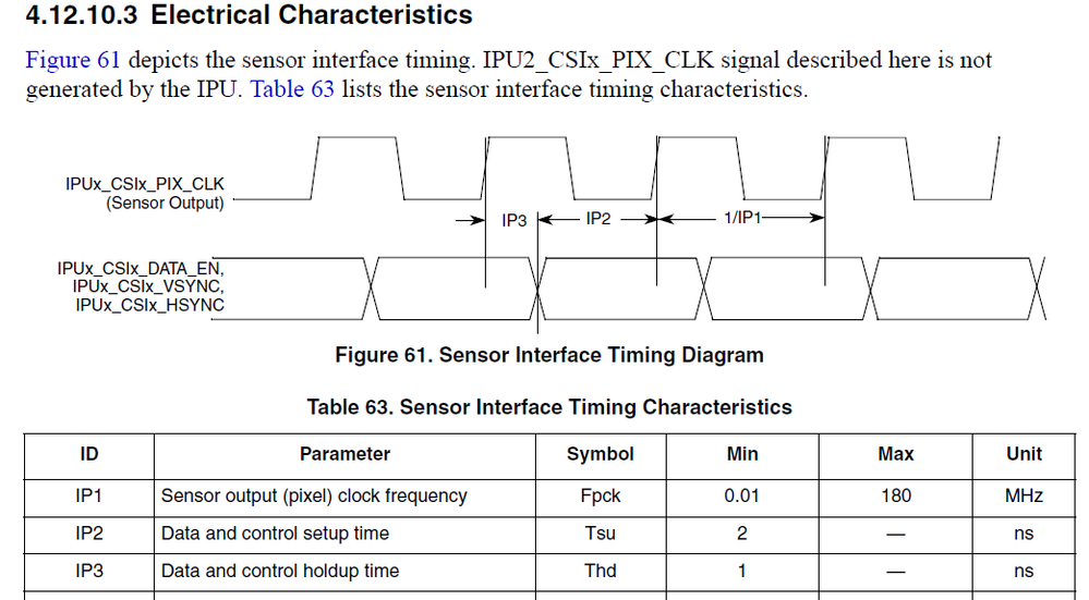
AC timing of IPUx_CSI input signals.
hello community,
I have some questions about AC timing of IPUx_CSI signals.
In datashee of i.MX6DQAEC, it have a timing characteristics of IPU CLK and DATA.
Which is a correct answer to major a each parameters.
1) Is start point of Tsu
1-1) center of the IPU_CSI_DATA signal? (OVDD*0.5)
1-2) Vih or Vil of the IPU_CSI_DATA signal? (OVDD*0.7) or (OVDD*0.3)
2) Is end of Tsu
2-1) center of the IPU_CSI_CLK signal? (OVDD*0.5)
2-2) Vih or Vil of the IPU_CSI_CLK signal? (OVDD*0.7) or (OVDD*0.3)
3) Is start point of Thd
3-1) center of the IPU_CSI_CLK signal? (OVDD*0.5)
3-2) Vih or Vil of the IPU_CSI_CLK signal? (OVDD*0.7) or (OVDD*0.3)
4) Is end point of Thd
3-1) center of the IPU_CSI_DATA signal? (OVDD*0.5)
3-2) Vih or Vil of the IPU_CSI_DATA signal? (OVDD*0.7) or (OVDD*0.3)
I am looking forward to hearing from you.
Best regards,
Ishii.
refer to the figure, tsu starts valid data signal, end referenced from a low-to-high transition of the pixel clock for 2:1, for CSI should be different mode, like gated mode, non-gated mode, for different mode, one can refer to the Reference Manual to get detailed information.
