- Forums
- Product Forums
- General Purpose MicrocontrollersGeneral Purpose Microcontrollers
- i.MX Forumsi.MX Forums
- QorIQ Processing PlatformsQorIQ Processing Platforms
- Identification and SecurityIdentification and Security
- Power ManagementPower Management
- Wireless ConnectivityWireless Connectivity
- RFID / NFCRFID / NFC
- Advanced AnalogAdvanced Analog
- MCX Microcontrollers
- S32G
- S32K
- S32V
- MPC5xxx
- Other NXP Products
- S12 / MagniV Microcontrollers
- Powertrain and Electrification Analog Drivers
- Sensors
- Vybrid Processors
- Digital Signal Controllers
- 8-bit Microcontrollers
- ColdFire/68K Microcontrollers and Processors
- PowerQUICC Processors
- OSBDM and TBDML
- S32M
- S32Z/E
-
- Solution Forums
- Software Forums
- MCUXpresso Software and ToolsMCUXpresso Software and Tools
- CodeWarriorCodeWarrior
- MQX Software SolutionsMQX Software Solutions
- Model-Based Design Toolbox (MBDT)Model-Based Design Toolbox (MBDT)
- FreeMASTER
- eIQ Machine Learning Software
- Embedded Software and Tools Clinic
- S32 SDK
- S32 Design Studio
- GUI Guider
- Zephyr Project
- Voice Technology
- Application Software Packs
- Secure Provisioning SDK (SPSDK)
- Processor Expert Software
- Generative AI & LLMs
-
- Topics
- Mobile Robotics - Drones and RoversMobile Robotics - Drones and Rovers
- NXP Training ContentNXP Training Content
- University ProgramsUniversity Programs
- Rapid IoT
- NXP Designs
- SafeAssure-Community
- OSS Security & Maintenance
- Using Our Community
-
- Cloud Lab Forums
-
- Knowledge Bases
- ARM Microcontrollers
- i.MX Processors
- Identification and Security
- Model-Based Design Toolbox (MBDT)
- QorIQ Processing Platforms
- S32 Automotive Processing Platform
- Wireless Connectivity
- CodeWarrior
- MCUXpresso Suite of Software and Tools
- MQX Software Solutions
- RFID / NFC
- Advanced Analog
-
- NXP Tech Blogs
- Home
- :
- i.MX Processors
- :
- i.MX Processors Knowledge Base
- :
- I.MX31 Using CLKO
I.MX31 Using CLKO
- Subscribe to RSS Feed
- Mark as New
- Mark as Read
- Bookmark
- Subscribe
- Printer Friendly Page
- Report Inappropriate Content
I.MX31 Using CLKO
I.MX31 Using CLKO
Using Clock Out - i.MX31PDK
i.MX31 has a clock out pin that can be used to output internal clock signals.
On the i.MX31PDK the clock out pin is accessible on TP1.
The clock out is controlled by register COSR (Clock Out Source Register) at address 0x53F8001C.
There three fields on COSR:
| Field | Description |
| CLKOEN (bit 9) | Clock output enable bit |
| CLKOUTDIV (bits 8-6) | Clock output divide factor |
| CLKOSEL (bits 3-0) | These bits select which clock is to be reflected on the clock output CKO. |
Here are the values each field may assume:
| CLKOEN Values | CLKOUTDIV Values | CLKOSEL Values |
1 clock output IO pin is enabled 0 clock output IO pin disabled | 000 => 1 001 => 2 010 => 4 011 => 8 100 => 16 | 0000 => mpl_dpdgck_clk 0001 => ipg_clk_ccm 0010 => upl_dpdgck_clk 0011 => pll_ref_clk 0100 => fpm_ckil512_clk 0101 => ipg_clk_ahb_arm 0110 => ipg_clk_arm 0111 => spl_dpdgck_clk 1000 => ckih 1001 => ipg_clk_ahb _emi_clk 1010 => ipg_clk_ipu_hsp 1011 => ipg_clk_nfc_20m 1100 => ipg_clk_perclk_uart1 1101 => ref_cir1 (ref_cir_gateload) 1110 => ref_cir2 (ref_cir_intrcload) 1111 => ref_cir3 (ref_cir_path) |
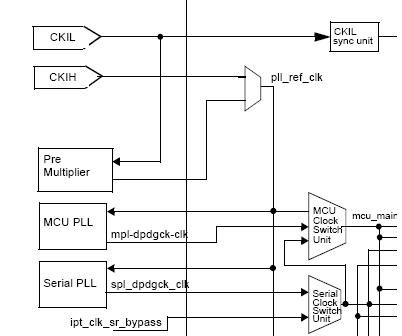
Based on the Clock Generation Scheme, we can play with COSR register using the
Register Accessing application to test Clock out pin by checking some i.MX31 internal clocks.
Testing
First we can check the value of CKIH, it should be 26MHz as a 26MHz is connected to that pin.
We can write 0x208 to COSR. [CLKOEN = 1| CLKOUTDIV = 1| CLKOSEL = ckih]
root@freescale /home$ ./io2 0x53f8001c w 0x208
/dev/mem opened.
Memory mapped on address 0x4001f000.
Written: 0x208
Then we can check pll_ref_clock.
We can write 0x203 to COSR. [CLKOEN = 1| CLKOUTDIV = 1| CLKOSEL = pll_ref_clk]
root@freescale /home$ ./io2 0x53f8001c w 0x203
/dev/mem opened.
Memory mapped on address 0x4001f000.
Written: 0x203
As expected, pll_ref_clock is equals to CKIH because CCMR[PCRS]=10.
- Reading CCMR to confirm CCMR[PCRS]=10:
root@freescale /home$ ./io2 0x53f80000
/dev/mem opened.
Memory mapped on address 0x4001f000.
Address value 0x53F80000 (0x4001f000): 0x174B0D7D
The pll_ref_clock inputs to MCU PLL and Serial PLL. We can check MCU PLL and Serial PLL configurations on MPCTL (0x53F80010) and SPCTL (0x53F80010) registers respectively.
- Reading MPCTL and SPCTL:
root@freescale /home$ ./io2 0x53f80010 /dev/mem opened. Memory mapped on address 0x4001f000. Address value 0x53F80010 (0x4001f010): 0x33280C | root@freescale /home$ ./io2 0x53f80018 /dev/mem opened. Memory mapped on address 0x4001f000. Address value 0x53F80018 (0x4001f018): 0x2072356 |
Determine the PLL multiplication factor from MPCTL and SPCTL:
- MPCTL: PD = 1 (0000) | MFD = 52 (0000110011) | MFI = 10 (1010) | MFN = 12 (0000001100)
- MCPTL Multiplication Factor: 20,46153
- mpl-dpdgck-clk = 20,46153 * 26MHz = 532 MHz
- SPCTL: PD = 1 (0000) | MFD = 520 (1000000111) | MFI = 8 (1000) | MFN = -170 (1101010110)
- SCPTL Multiplication Factor: 15,3461538
- spl-dpdgck-clk = 15,3461538 * 26MHz = 399 MHz
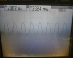
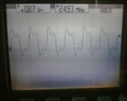
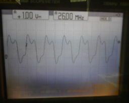
Finally we can output mpl-dpdgck-clk and spl_dpdgck_clk values to check the calculations above.
We can write 0x300 to COSR for mpl-dpdgck-clk. [CLKOEN = 1| CLKOUTDIV = 16| CLKOSEL = mpl_dpdgck_clk]
And 0x307 for spl-dpdgck-clk. [CLKOEN = 1| CLKOUTDIV = 16| CLKOSEL = spl_dpdgck_clk]
root@freescale /home$ ./io2 0x53f8001c w 0x300 /dev/mem opened. Memory mapped on address 0x4001f000. Written: 0x300 | root@freescale /home$ ./io2 0x53f8001c w 0x307 /dev/mem opened. Memory mapped on address 0x4001f000. Written: 0x307 |
 |  |
By multiplying the results above by 16 to compensate for CLKOUTDIV we have the expected results.


