- Forums
- Product Forums
- General Purpose MicrocontrollersGeneral Purpose Microcontrollers
- i.MX Forumsi.MX Forums
- QorIQ Processing PlatformsQorIQ Processing Platforms
- Identification and SecurityIdentification and Security
- Power ManagementPower Management
- MCX Microcontrollers
- S32G
- S32K
- S32V
- MPC5xxx
- Other NXP Products
- Wireless Connectivity
- S12 / MagniV Microcontrollers
- Powertrain and Electrification Analog Drivers
- Sensors
- Vybrid Processors
- Digital Signal Controllers
- 8-bit Microcontrollers
- ColdFire/68K Microcontrollers and Processors
- PowerQUICC Processors
- OSBDM and TBDML
-
- Solution Forums
- Software Forums
- MCUXpresso Software and ToolsMCUXpresso Software and Tools
- CodeWarriorCodeWarrior
- MQX Software SolutionsMQX Software Solutions
- Model-Based Design Toolbox (MBDT)Model-Based Design Toolbox (MBDT)
- FreeMASTER
- eIQ Machine Learning Software
- Embedded Software and Tools Clinic
- S32 SDK
- S32 Design Studio
- GUI Guider
- Zephyr Project
- Voice Technology
- Application Software Packs
- Secure Provisioning SDK (SPSDK)
- Processor Expert Software
- MCUXpresso Training Hub
-
- Topics
- Mobile Robotics - Drones and RoversMobile Robotics - Drones and Rovers
- NXP Training ContentNXP Training Content
- University ProgramsUniversity Programs
- Rapid IoT
- NXP Designs
- SafeAssure-Community
- OSS Security & Maintenance
- Using Our Community
-
- Cloud Lab Forums
-
- Knowledge Bases
Hi,
Is there an alternative location QN9020 look for NVDS data apart from 0x30000000? I have verified using JLink I can read the NVDS data from the QN9020 MiniDK board from location 0x30000000. But when I do it from the internal board it, returns all 0 for at least about 0x1000 locations. But if I read the data using NVDS configurator the tool can read the value. So the system does have access to the nvds data. But not clear where is it reading from!
已解决! 转到解答。
Hi Tony,
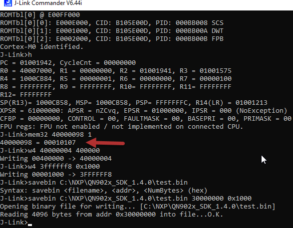
What is the value of the register that you readout? 40000098
Power on flash: see register 40000098 value, mem32 40000098 1
if bit 2 is to 0, set bit 2 to 1, saving the previous values of the register.
Regards,
Mario
Hi Tony,
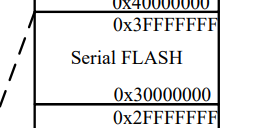
As you know, the 0x30000000 is the direction of the serial Flash begins.
What do you mean with the But when I do it from the internal board it? Did you try to read using the nvds_get()?
Regards,
Mario
Is there any document which describes how to read and write onto the internal flash using JLink? I have the commands on how to read the memory from your post in the other thread. But not sure what the steps are to write into the flash. Also any documents which describes addresses like 0x3ffffff8 would be useful.
Although I tried
w4 3ffffff8 0x4 #[Tried without this line too]
w4 30000008 0xa5a5a5a5
it did not work.
Is there any other document which details the internal flash? Section 9.2 of data sheet, states the interface is internal SPI. I am guessing this is not one of the SPI [0/1]detailed in 9.4.2 of data sheet? Does the internal SPI needs to initialised from the user code?
Hi Tony,
Remember, that the QN9020 is waiting for ISP commands in the case that you want to write using UART or SPI.
Are you trying to read out all the memory flash?
Could you please explain with more details what is your final application?
Regards,
Mario
I am trying to read the nvds section to check for any corruption [Please see comment on this thread 24-Dec-2019 02:44]. As I cant verify the data was checking whether I could write to the flash using JLink.
The application is a GATT based BLE application.
Hi Tony,
As you know, the QN9020 has Integrated 32-bit Arm® Cortex® M0 MCU. The commands for writing are the same using JLink. Be sure that the device is not in ISP mode.
Also, look at the UM10995 for the ISP commands.
Regards,
Mario
Hi Mario,
Can you please have a look whether the steps in reading the nvds data are correct. As you can see, I cant read the data using JLink. But can using the NVDS Configurator.
Note: I reset the board before the start and just after starting "QBlue NVDS Configurator" [About 2:00 on the video].
Hi Tony,
What is the value of the register that you readout? 40000098
Power on flash: see register 40000098 value, mem32 40000098 1
if bit 2 is to 0, set bit 2 to 1, saving the previous values of the register.
Regards,
Mario
I am reading from the internal board, using JlLink(same steps I use to read from QN9020 MIniDk Board).The internal board I mentioned is one of our internal development boards with QN9020. With JLink when I save the data using
savebin C:\path\data.bin 0x30000000 0x1000, it is all 0.
I dont think it is something to do with JLink because I can read the BLE Processor memory 0x2E000000 and get data which i recognise.
But after the above step, if I use NVDS Configurator tool to check the data, it reads the data over UART without any error. All the NVDS data are there intact.
Not sure what is different. So am presuming
- either the JLink read somehow failed or
- the NVDS Configurator is accessing the memory from another location?

