
- Forums
- Product Forums
- General Purpose MicrocontrollersGeneral Purpose Microcontrollers
- i.MX Forumsi.MX Forums
- QorIQ Processing PlatformsQorIQ Processing Platforms
- Identification and SecurityIdentification and Security
- Power ManagementPower Management
- Wireless ConnectivityWireless Connectivity
- RFID / NFCRFID / NFC
- Advanced AnalogAdvanced Analog
- Neural Processing UnitsNeural Processing Units
- MCX Microcontrollers
- S32G
- S32K
- S32V
- MPC5xxx
- Other NXP Products
- S12 / MagniV Microcontrollers
- Powertrain and Electrification Analog Drivers
- Sensors
- Vybrid Processors
- Digital Signal Controllers
- 8-bit Microcontrollers
- ColdFire/68K Microcontrollers and Processors
- PowerQUICC Processors
- OSBDM and TBDML
- S32M
- S32Z/E
-
- Solution Forums
- Software Forums
- MCUXpresso Software and ToolsMCUXpresso Software and Tools
- CodeWarriorCodeWarrior
- MQX Software SolutionsMQX Software Solutions
- Model-Based Design Toolbox (MBDT)Model-Based Design Toolbox (MBDT)
- FreeMASTER
- eIQ Machine Learning Software
- Embedded Software and Tools Clinic
- S32 SDK
- S32 Design Studio
- GUI Guider
- Zephyr Project
- Voice Technology
- Application Software Packs
- Secure Provisioning SDK (SPSDK)
- Processor Expert Software
- Generative AI & LLMs
-
- Topics
- Mobile Robotics - Drones and RoversMobile Robotics - Drones and Rovers
- NXP Training ContentNXP Training Content
- University ProgramsUniversity Programs
- Rapid IoT
- NXP Designs
- SafeAssure-Community
- OSS Security & Maintenance
- Using Our Community
-
- Cloud Lab Forums
-
- Knowledge Bases
- ARM Microcontrollers
- i.MX Processors
- Identification and Security
- Model-Based Design Toolbox (MBDT)
- QorIQ Processing Platforms
- S32 Automotive Processing Platform
- Wireless Connectivity
- CodeWarrior
- MCUXpresso Suite of Software and Tools
- MQX Software Solutions
- RFID / NFC
- Advanced Analog
- Neural Processing Units
-
- NXP Tech Blogs
- Home
- :
- QorIQプロセッシングプラットフォーム
- :
- Tシリーズ
- :
- Re: T1022 Boot issue
T1022 Boot issue
- RSS フィードを購読する
- トピックを新着としてマーク
- トピックを既読としてマーク
- このトピックを現在のユーザーにフロートします
- ブックマーク
- 購読
- ミュート
- 印刷用ページ
T1022 Boot issue
- 新着としてマーク
- ブックマーク
- 購読
- ミュート
- RSS フィードを購読する
- ハイライト
- 印刷
- 不適切なコンテンツを報告
Hello,
We are using T1022NSN7W in our design. We give PORESET_B as low for 400ms. CFG_RCW_SRC0 TO CFG_RCW_SRC8 is set to 0x9E (Hardcoded). But when we probe HRESET_B is coming low and ASLEEP is coming high. What could be the issue.
- 新着としてマーク
- ブックマーク
- 購読
- ミュート
- RSS フィードを購読する
- ハイライト
- 印刷
- 不適切なコンテンツを報告
When we try to bring system up using lauterbach tool by running. cmm file then system comes up and we can read registers SVR PVR and others but not coming up with following two cases :
1. When doing hardcoded (9E) system is not coming up.
2. And also when configuring as SPI boot, the clock, CS, MISO MOSI transactions are seen but processor is not able to boot up.
3. When accessing using lauterbach we are able to bring system up, In this case can we say :
a) RCW configuration is ok and
b) reset sequence is ok,
c) System power is ok
d) SYSCLK is ok.
Please advice...
- 新着としてマーク
- ブックマーク
- 購読
- ミュート
- RSS フィードを購読する
- ハイライト
- 印刷
- 不適切なコンテンツを報告
Comments:
1. Is it a new design? How many boards have been built? How high is the failure rate?
2. Please provide the schematic.
3. Please provide the waveform that you have measured, such as ASLEEP, PORESET_B, SYSCLK on the same screen and can illustrate their timing relationship and signal integrity.
- 新着としてマーク
- ブックマーク
- 購読
- ミュート
- RSS フィードを購読する
- ハイライト
- 印刷
- 不適切なコンテンツを報告
Apology for delayed response. Please find response inline :
1. Is it a new design? How many boards have been built? How high is the failure rate?
RESPONSE : Yes, it's a new design. 10 boards are assembled. We have tested on four boards.
2. Please provide the schematic.
RESPONSE : PFA processor schematic.
3. Please provide the waveform that you have measured, such as ASLEEP, PORESET_B, SYSCLK on the same screen and can illustrate their timing relationship and signal integrity.
RESPONSE : PFA waveforms. Snapshot '1' shows ASLEEP (Blue color) and PORESET_B(Yellow color).Snapshot '2' shows clock(Pink) and PORESET_B (Yellow color).
- 新着としてマーク
- ブックマーク
- 購読
- ミュート
- RSS フィードを購読する
- ハイライト
- 印刷
- 不適切なコンテンツを報告
NXP is trying to help the customer, so please request the customer to release the material that let other people outside C-dot can make them useful.
Comments
- Please capture the waveform that can illustrate the relationship between SoC signals. For example, search "power-on reset sequence" at the RM. Existing waveform cannot reveal the status.
- How is failure rate?
- Please generate a schematic that is text searchable. It is not possible to check relevant connections without searching with keyword.
- 新着としてマーク
- ブックマーク
- 購読
- ミュート
- RSS フィードを購読する
- ハイライト
- 印刷
- 不適切なコンテンツを報告
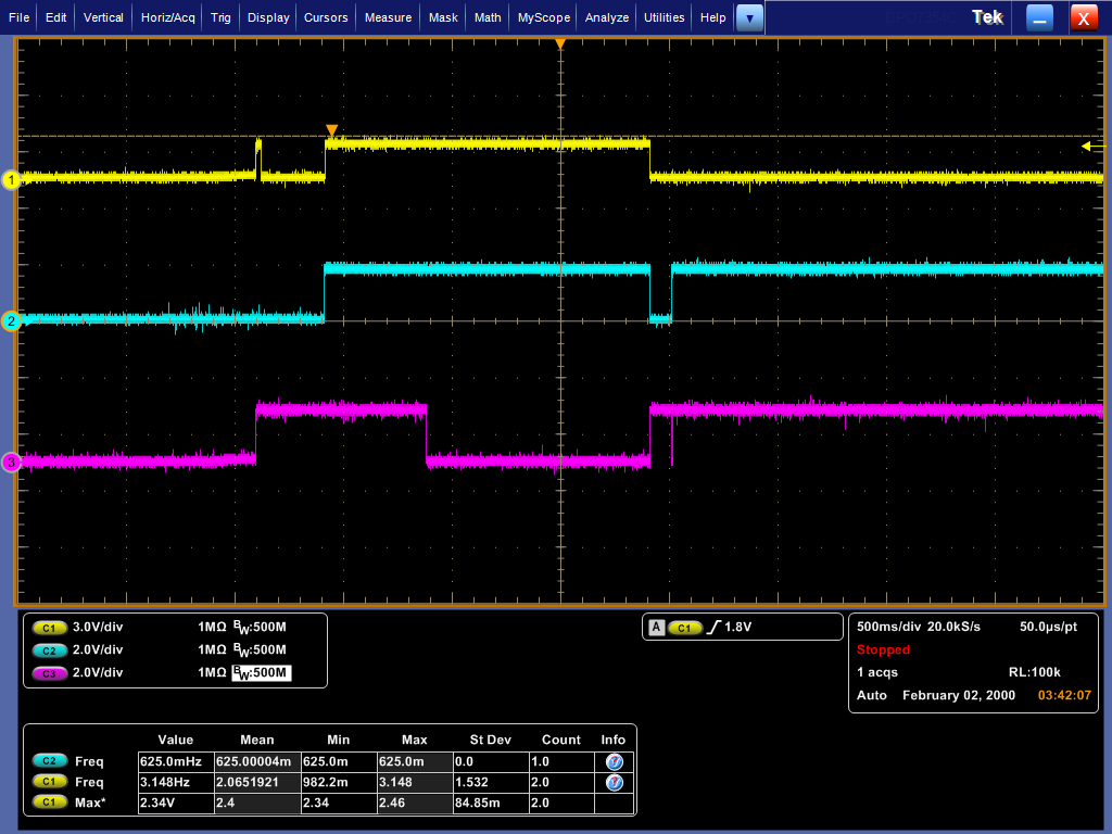
- Please capture the waveform that can illustrate the relationship between SoC signals. For example, search "power-on reset sequence" at the RM. Existing waveform cannot reveal the status. RESPONSE : Please find attached clk,poreset and hreset in one frame capture. Yellow is HRESET, BLUE is PORESET and PINK is diff_sysclk.
- How is failure rate? RESPONSE : Four cards, out of these 3 are completely failing to boot, one card boots 90% times and 10% times it fails.
- Please generate a schematic that is text searchable. It is not possible to check relevant connections without searching with keyword. RESPONSE : Please find attached.
- 新着としてマーク
- ブックマーク
- 購読
- ミュート
- RSS フィードを購読する
- ハイライト
- 印刷
- 不適切なコンテンツを報告
EVT0_B must be pulled up. If it is not pulled up, it may affect normal boot up.
Please rework the board to confirm it.
- 新着としてマーク
- ブックマーク
- 購読
- ミュート
- RSS フィードを購読する
- ハイライト
- 印刷
- 不適切なコンテンツを報告
I double checked the datasheet, EVT0 has internal weak pull up, but others EVT pins haven't specified.
At the board, EVT0,1,4 are not externally pulled up. So please pull them up through 2-10k ohm resistors, individually, including EVT0_B.
Some more comments:
- Please check for any difference between good and failed conditions. Zoom in and capture, if you found any difference.
- What is the power up sequencing? Is GVDD ramp last and PORESET deassert after GVDD becomes nominal?
- How is TRST_B asserted? Is it sync with PORESET_B? Check the CPLD equation or confirm with waveform capture.
- 新着としてマーク
- ブックマーク
- 購読
- ミュート
- RSS フィードを購読する
- ハイライト
- 印刷
- 不適切なコンテンツを報告
1. At the board, EVT0,1,4 are not externally pulled up. So please pull them up through 2-10k ohm resistors, individually, including EVT0_B.
RESPONSE : There is no pinout on EVT0,1,4 pins in our board. EVT2 and EVT3 are pulled up on board. We have used T1022 in our other designs also where EVT0,1,4 are left floating and designs are working.
2. Please check for any difference between good and failed conditions. Zoom in and capture, if you found any difference.
RESPONSE : We are working on this.
3. What is the power up sequencing? Is GVDD ramp last and PORESET deassert after GVDD becomes nominal?
RESPONSE : After G1VDD rampup , there is time of 500ms approx and PORESET deassert.
4. How is TRST_B asserted? Is it sync with PORESET_B? Check the CPLD equation or confirm with waveform capture.
RESPONSE : Earlier CPLD equation was : PROC_TRST_N<=COP_TRST_N;
Now, we have changed this to : PROC_TRST_N <= porest_extended and COP_TRST_N;
Also, PROC_PORST_N <= porest_extended and COP_HRESET_N;
Query : We have seen that when we access via JTAG(run rcw.cmm file and then do system up and in target reset), COP_HRESET_N is driven low twice with pulse width of 50ms and gap of around 1.5s between these two pulses. Do we need to replicate this scenario for PROC_PORST_N also. As of now we are giving only single pulse of 400ms.
- 新着としてマーク
- ブックマーク
- 購読
- ミュート
- RSS フィードを購読する
- ハイライト
- 印刷
- 不適切なコンテンツを報告
Please illustrate the TRST modification/query with waveform. Hand-drafting is OK.
Misunderstanding will happen with text description.
- 新着としてマーク
- ブックマーク
- 購読
- ミュート
- RSS フィードを購読する
- ハイライト
- 印刷
- 不適切なコンテンツを報告
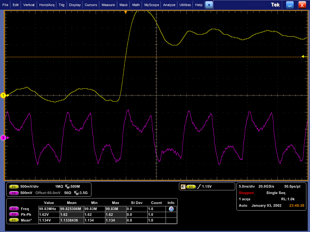
1. Please find attached waveform for Query :
CASE1 : RCW configuration via JTAG : "Hardreset_poreset_JTAGexecution.png". Yellow is PROC_HRESET_N. and Blue is COP_HRESET_N. We run rcw.cmm file in trace32 and capture COP_HRESET_N signal transition.
CASE2 : RCW via SPI boot : "Hardreset_poreset_spiboot.png". We change PROC_PORESET_N to behave similar to COP_HRESET_N to simulate same behaviour. In this case, PROC_HRESET_N comes high first time but never comes high during second time.
2. "poreset_proc_trst_nduring powerup.png" PFA snapshot of PROC_TRST_N on modificaiton. It follows PROC_PORESET_N on modification. PROC_TRST_N is pulled up on JTAG connector.
PROC_TRST_N <= porest_extended and COP_TRST_N;
Earlier it was : PROC_TRST_N <= COP_TRST_N;
Anyways, we didn't see any transition on COP_TRST_N during access via JTAG also, so this mayn't affect functionality during processor boot from SPI.
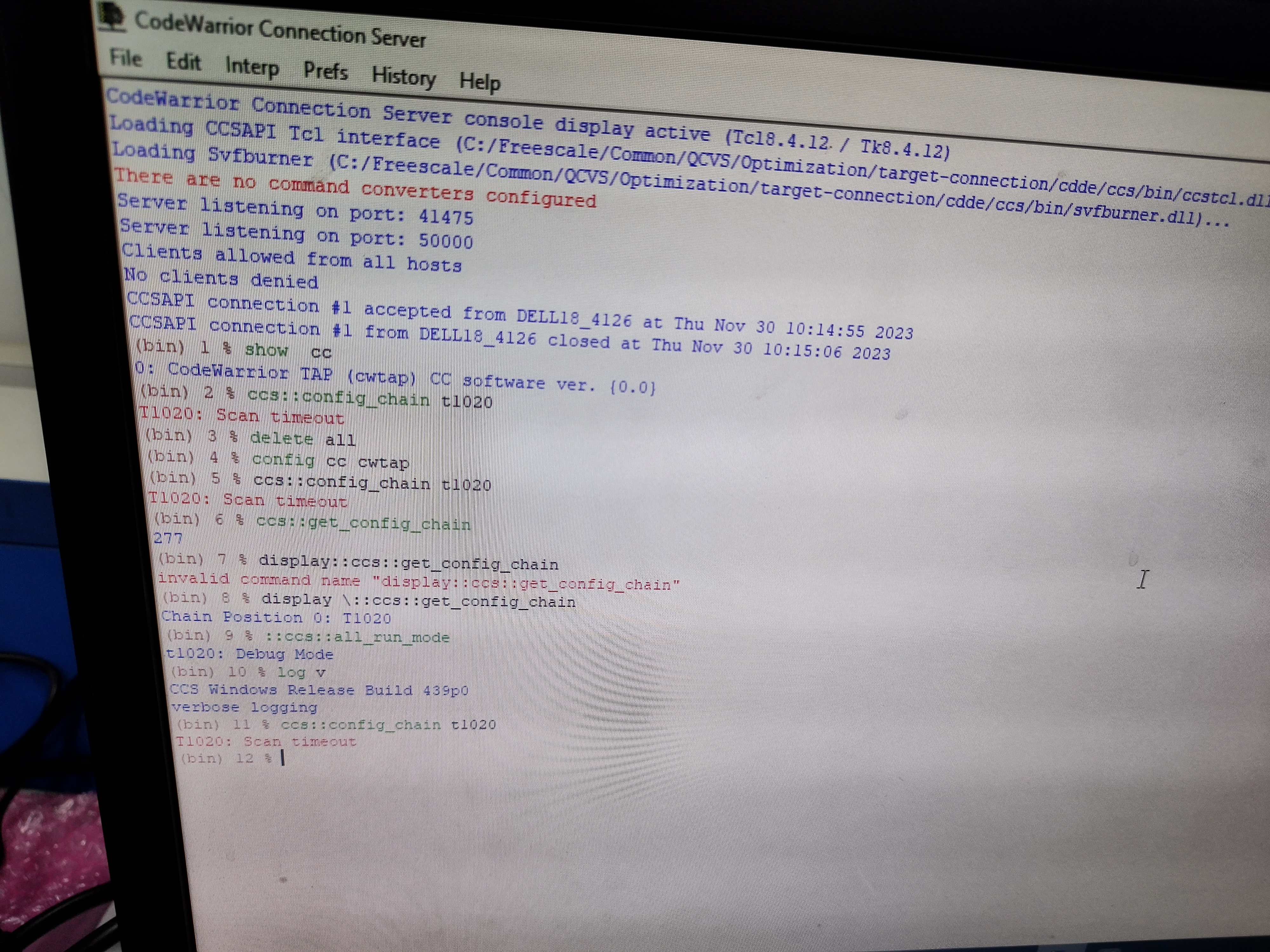
3. In one card which is booting 90% times, that card was getting stuck at DDR, so we were trying to connect Code Warrior Tool with JTAG but issue is Tool is not scanning the processor. "Board scan" command is running successful(didn't take snapshot for board scan cmd) but scan chain cmd fails to scan and gives timeout error. PFA snapshot for same. Code Warrior cmds.jpg and Code Warrior.jpg.
- 新着としてマーク
- ブックマーク
- 購読
- ミュート
- RSS フィードを購読する
- ハイライト
- 印刷
- 不適切なコンテンツを報告
Regarding to the capture "Hardreset_porest_spiboot.png", it does not look normal.
Please capture the waveform that can illustrate the relationship between SoC signals. For example, search "power-on reset sequence" at the RM. Existing waveforms cannot reveal the status. Suggest to include ASLEEP.
- 新着としてマーク
- ブックマーク
- 購読
- ミュート
- RSS フィードを購読する
- ハイライト
- 印刷
- 不適切なコンテンツを報告
- 新着としてマーク
- ブックマーク
- 購読
- ミュート
- RSS フィードを購読する
- ハイライト
- 印刷
- 不適切なコンテンツを報告
Could you label the signal? Anyway, they cannot match to whatever SoC required. PORESET_B should be monotonic low to high at the power up. i.e. Keep low before all voltage rails ramp, until GVDD becomes nominal. No toggling, just single low to high at POR. Suggest to compare the previous produced board. What circuit/component has been modified? Please clean up the reset signal if previous board also has got similar problem.
- 新着としてマーク
- ブックマーク
- 購読
- ミュート
- RSS フィードを購読する
- ハイライト
- 印刷
- 不適切なコンテンツを報告
Will update later.
- 新着としてマーク
- ブックマーク
- 購読
- ミュート
- RSS フィードを購読する
- ハイライト
- 印刷
- 不適切なコンテンツを報告
If getting DDR working is the first priority, I suggest focusing on the DDR. JTAG signal integrity is not good.
Please set the verbosity to maximum and dump the u-boot log. Please dump the DDR register in full range.
- 新着としてマーク
- ブックマーク
- 購読
- ミュート
- RSS フィードを購読する
- ハイライト
- 印刷
- 不適切なコンテンツを報告
we have added:#define DEBUGin following files:1. u-boot/board/freescale/t104xrdb/ddr.c2. u-boot//drivers/ddr/fsl/ctrl_regs.c3. u-boot/drivers/ddr/fsl/main.c4. u-boot/drivers/ddr/fsl/options.c5. u-boot/drivers/ddr/fsl/fsl_ddr_gen4.c6. u-boot/drivers/ddr/fsl/ddr4_dimm_params.c7. u-boot/drivers/ddr/fsl/lc_common_dimm_params.c8. u-boot/drivers/ddr/fs/interactive.c
UBOOT LOG 1 :
- 新着としてマーク
- ブックマーク
- 購読
- ミュート
- RSS フィードを購読する
- ハイライト
- 印刷
- 不適切なコンテンツを報告
Please use QCVS DDRv tool to do DDR optimization and validation.
- 新着としてマーク
- ブックマーク
- 購読
- ミュート
- RSS フィードを購読する
- ハイライト
- 印刷
- 不適切なコンテンツを報告
As also said earlier ,
In one card which is booting 90% times, that card was getting stuck at DDR, so we were trying to connect Code Warrior Tool with JTAG but issue is Tool is not scanning the processor. "Board scan" command is running successful(didn't take snapshot for board scan cmd) but scan chain cmd fails to scan and gives timeout error. PFA snapshot for same. Code Warrior cmds.jpg and Code Warrior.jpg.
- 新着としてマーク
- ブックマーク
- 購読
- ミュート
- RSS フィードを購読する
- ハイライト
- 印刷
- 不適切なコンテンツを報告
Please configure the target board as hard-coded RCW to check whether "ccs::config_chain t1020" can be executed successfully.
If still no, it means there is JTAG interface hardware design issue. Please refer to "Figure 25. JTAG interface connection" in AN4825.
- 新着としてマーク
- ブックマーク
- 購読
- ミュート
- RSS フィードを購読する
- ハイライト
- 印刷
- 不適切なコンテンツを報告
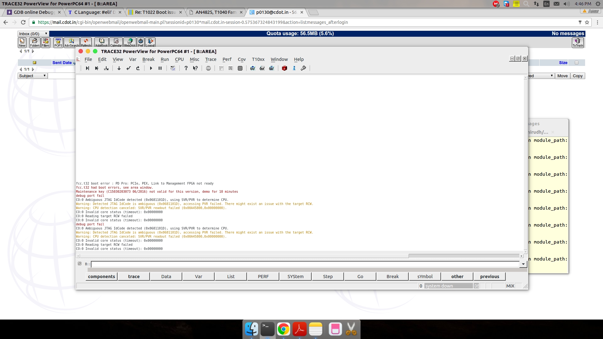
In one of card (card number 69) , we have configured as HARDCODED 9E, but still processor doesn't come up and shows following error in message of lauterbach tool. "HARDCODED_CPUSettings_InTargetReset"
Also, when we verify by running RCW.cmm in tool and then read the DCPC registers, the RCW_SRC is read as 9E. Also, we have observed that this 9E toggle between 9E and 9F sometimes. Although it's actually set to 9E. Two snapshots for this : 1. HARDCODED_run RCWcmm_CPUSettings_InTargetReset and 2. DCPC when Hardcoded_runRCWcmm_CPUSettings_InTargetReset
PFA images snapshots.
If still no, it means there is JTAG interface hardware design issue. Please refer to "Figure 25. JTAG interface connection" in AN4825.
RESPONSE : We are able to program and verify the SPI flash.
We are able to program and verify NAND Flash.
We are succesfully able to run RCW.cmm and bring processor up and do in-Target-Reset when configured 45h(SPI Boot) and it is always consistently successful.