
- Forums
- Product Forums
- General Purpose MicrocontrollersGeneral Purpose Microcontrollers
- i.MX Forumsi.MX Forums
- QorIQ Processing PlatformsQorIQ Processing Platforms
- Identification and SecurityIdentification and Security
- Power ManagementPower Management
- Wireless ConnectivityWireless Connectivity
- RFID / NFCRFID / NFC
- Advanced AnalogAdvanced Analog
- MCX Microcontrollers
- S32G
- S32K
- S32V
- MPC5xxx
- Other NXP Products
- S12 / MagniV Microcontrollers
- Powertrain and Electrification Analog Drivers
- Sensors
- Vybrid Processors
- Digital Signal Controllers
- 8-bit Microcontrollers
- ColdFire/68K Microcontrollers and Processors
- PowerQUICC Processors
- OSBDM and TBDML
- S32M
- S32Z/E
-
- Solution Forums
- Software Forums
- MCUXpresso Software and ToolsMCUXpresso Software and Tools
- CodeWarriorCodeWarrior
- MQX Software SolutionsMQX Software Solutions
- Model-Based Design Toolbox (MBDT)Model-Based Design Toolbox (MBDT)
- FreeMASTER
- eIQ Machine Learning Software
- Embedded Software and Tools Clinic
- S32 SDK
- S32 Design Studio
- GUI Guider
- Zephyr Project
- Voice Technology
- Application Software Packs
- Secure Provisioning SDK (SPSDK)
- Processor Expert Software
- Generative AI & LLMs
-
- Topics
- Mobile Robotics - Drones and RoversMobile Robotics - Drones and Rovers
- NXP Training ContentNXP Training Content
- University ProgramsUniversity Programs
- Rapid IoT
- NXP Designs
- SafeAssure-Community
- OSS Security & Maintenance
- Using Our Community
-
- Cloud Lab Forums
-
- Knowledge Bases
- ARM Microcontrollers
- i.MX Processors
- Identification and Security
- Model-Based Design Toolbox (MBDT)
- QorIQ Processing Platforms
- S32 Automotive Processing Platform
- Wireless Connectivity
- CodeWarrior
- MCUXpresso Suite of Software and Tools
- MQX Software Solutions
- RFID / NFC
- Advanced Analog
-
- NXP Tech Blogs
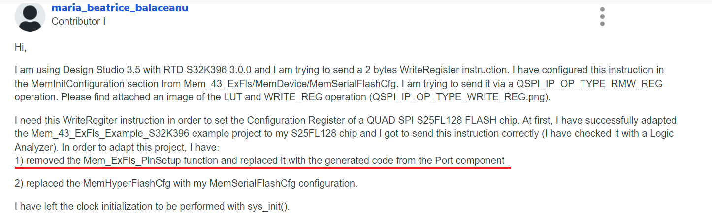
Hi,
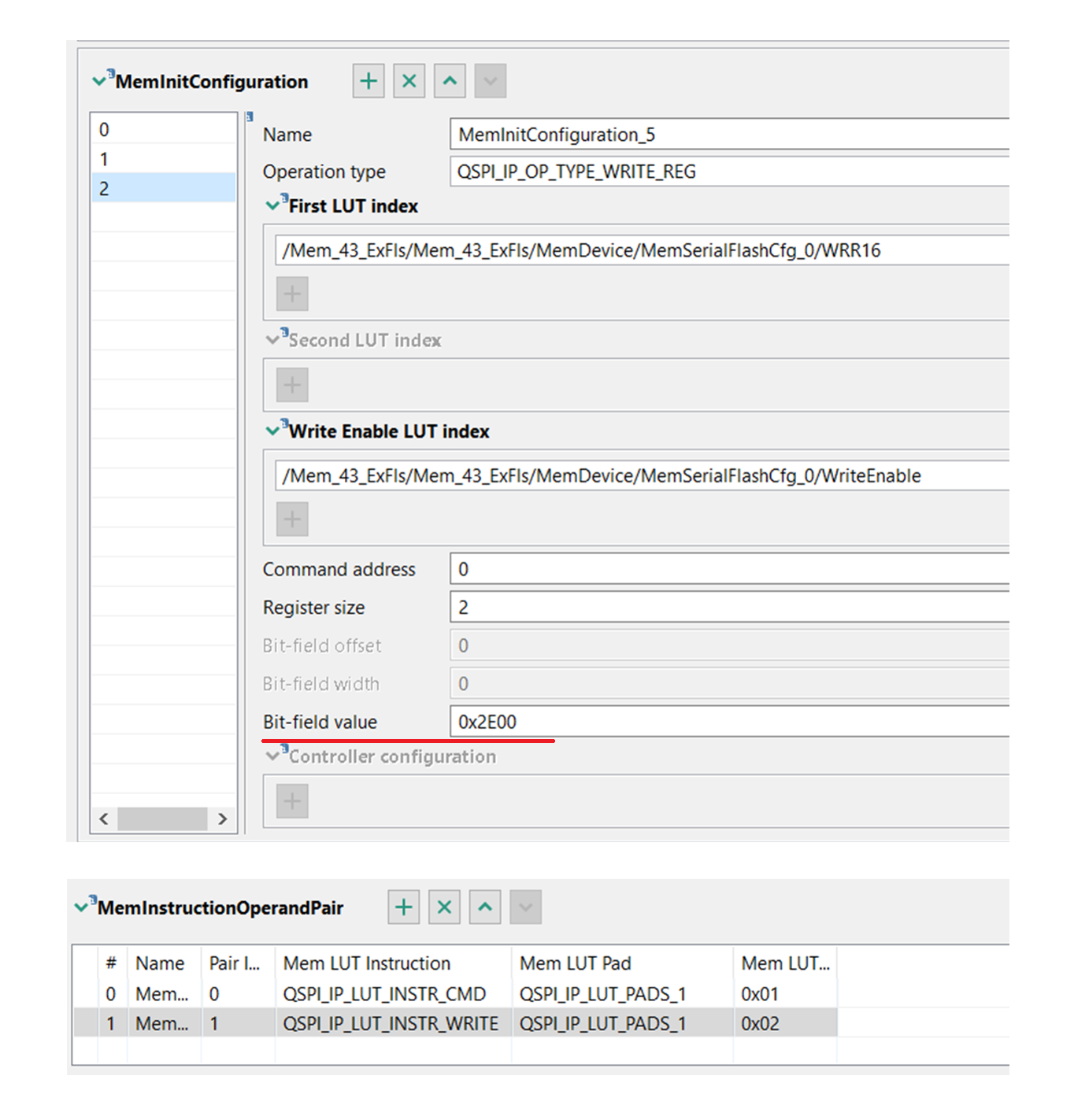
I am using Design Studio 3.5 with RTD S32K396 3.0.0 and I am trying to send a 2 bytes WriteRegister instruction. I have configured this instruction in the MemInitConfiguration section from Mem_43_ExFls/MemDevice/MemSerialFlashCfg. I am trying to send it via a QSPI_IP_OP_TYPE_RMW_REG operation. Please find attached an image of the LUT and WRITE_REG operation (QSPI_IP_OP_TYPE_WRITE_REG.png).
I need this WriteRegiter instruction in order to set the Configuration Register of a QUAD SPI S25FL128 FLASH chip. At first, I have successfully adapted the Mem_43_ExFls_Example_S32K396 example project to my S25FL128 chip and I got to send this instruction correctly (I have checked it with a Logic Analyzer). In order to adapt this project, I have:
1) removed the Mem_ExFls_PinSetup function and replaced it with the generated code from the Port component
2) replaced the MemHyperFlashCfg with my MemSerialFlashCfg configuration.
I have left the clock initialization to be performed with sys_init().
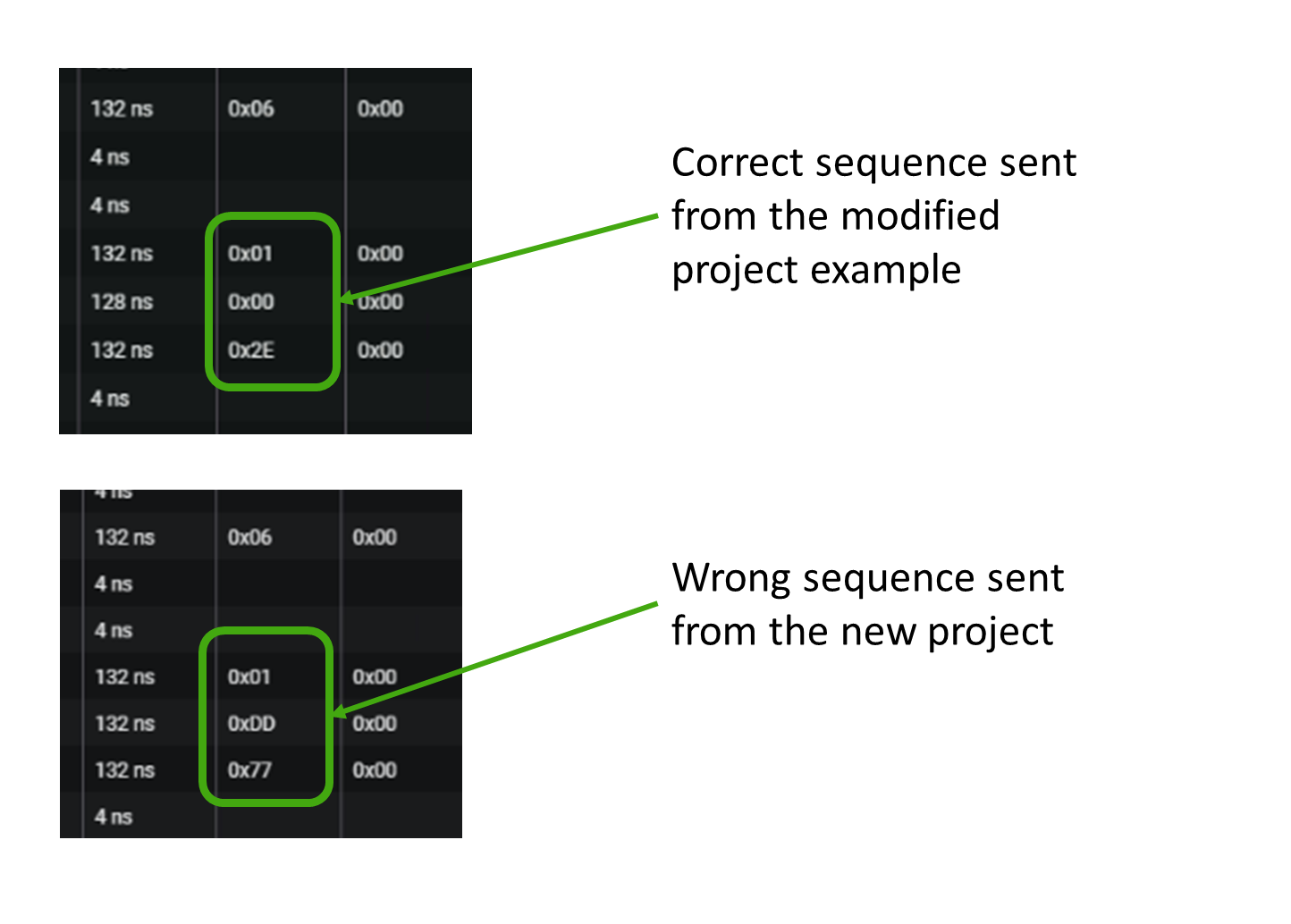
However, when I tried to integrate the same Serial Flash and QSPI_IP_OP_TYPE_RMW_REG configurations into a new project (which uses the generated code for initializing the clocks and contains some additional modules such as Platform, SPI, CAN, etc.), it ends up sending completely different values than the ones set in the "Bit-field value" field. I have attached a comparison between what shows up on the Logic Analyzer for the modified project and for the new one (Logic_Analyzer_Data.png). The other QSPI instructions (write Enable 0x06, Read Status Register 0x05, Read Configuration Register 0x35) seem to be sent correctly.
Is there anything I need to configure in order to send the two bytes WriteRegister instruction correctly?
Thank you in advance,
Beatrice
已解决! 转到解答。
Hi @maria_beatrice_balaceanu ,
I've just realized that a part of divider of MUX_10_DC done default by HW, so, we don't need to plus it to MUX_10_DC_DIV. So, it is not bug in driver. So, can you please cancel request to hotfix.
Just follow RM with option A+ memory


In DS configuration:


Best regards,
Nhi
Hi, Nhi Nguyen,
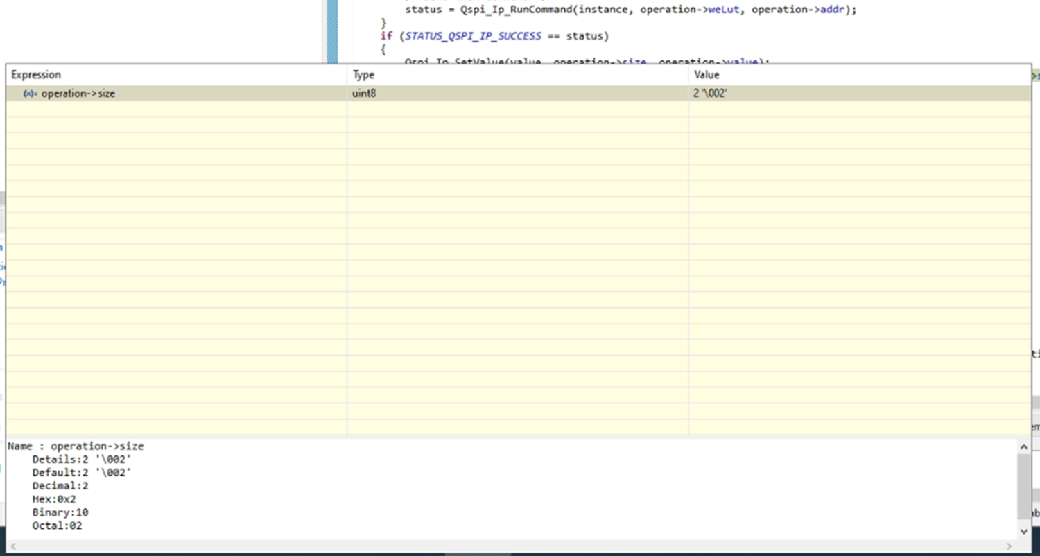
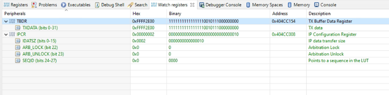
Thank you! I have checked the "value" and "operation->size" fields and they seem to match the ones configured in QSPI_IP_OP_TYPE_RMW_REG (1_WriteReg_value.png and 2_WriteReg_size). I have also checked the values of the IPCR and TBDR registers after exiting Mem_43_ExFls_Init(). The values are in 3_RegistersVals.png.
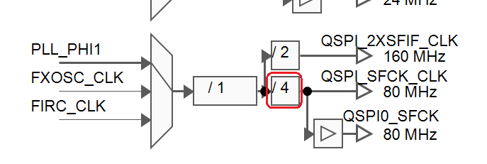
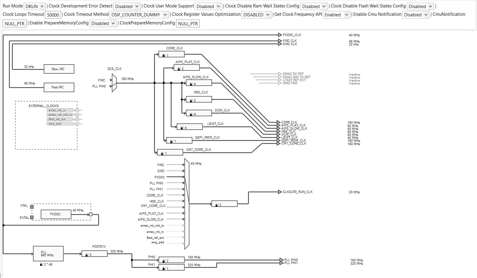
Could the clock configuration have any influence on the way the data from these registers is transmitted? I have attached the clock configuration in 4_clock_conf.png and 5_clock_conf.png. Please note that, for 5_clock_conf, Design Studio does not allow me to modify the divider of QSPI_SFCK_CLK (marked with red).
Thank you,
Beatrice
Hi maria_beatrice_
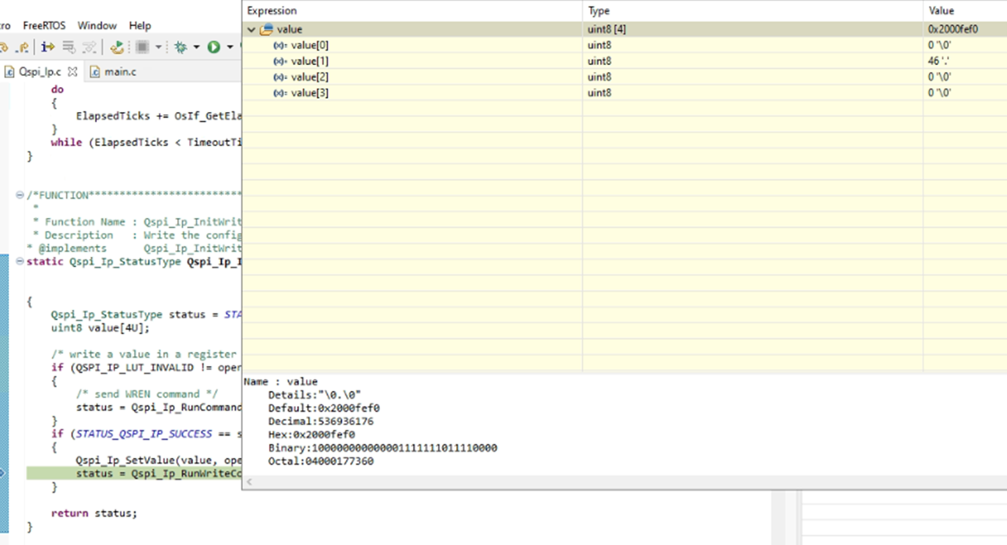
Can you read value of this variable "value" that I highlighted in red in below picture:

This "value" will store value configured by the parameter "Bit-field value" in configuration. Then, data transferred into Tx buffer through the register TX Buffer Data Register(TBDR) and size of data determined in the register IP Configuration Register (IPCR). So, Can you please capture value of 2 these registers after you run over the function Mem_43_ExFls_Init()?
Best regards,
Nhi
Hi maria_beatrice_
Because you said that you can send successful one byte so I don't think it come from clock. And clocks like: QSPI_MEM_CLK , QSPI_SFCK,... you just need to use it default from configuration. I saw that they was satisfied range of clocks. I didn't see affect to data also. But, it's strange because data is written into TDBR correctly and you measured signals at output of MCU.
I prefer that this issue can come from Port. My suggestion to find where the issue can come from :

You can try to use 1 of your first project instead of 1 in your second project. Then, point 2.
Best regards,
Nhi
Hi, Nhi Nguyen,
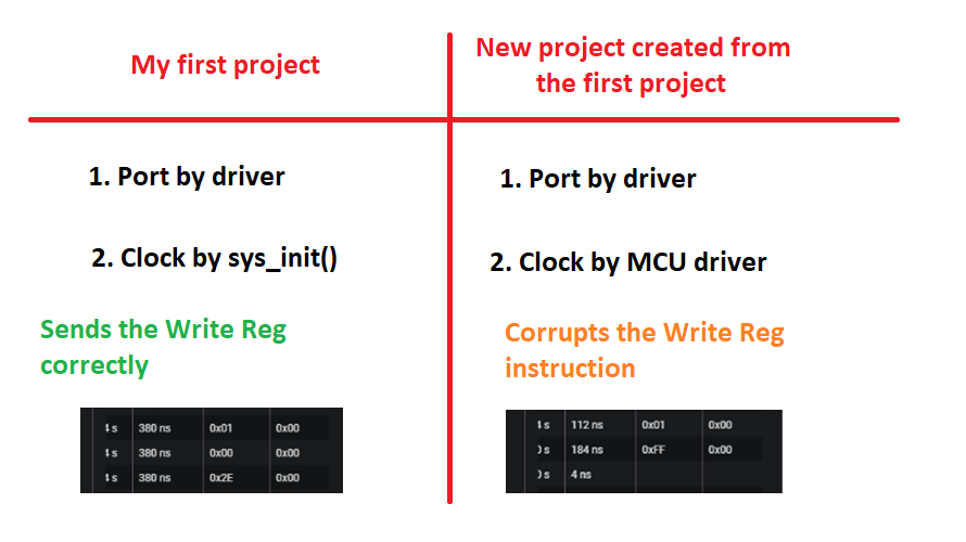
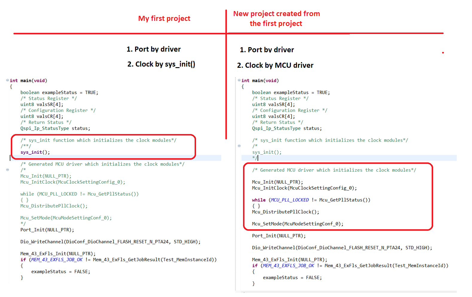
Actually, my modified example (the first project) contains the port initialization from the generated driver (as I have mentioned in the request: 1_msg_port_comp.png).
Thank you for your suggestion related to the configuration of the project! In order to remove any possible influence of other modules, I have created another project from the modified example which worked. For this new project, I have replaced sys_init() with the MCU driver. Now, it seems that this new project isn't sending the correct instruction either. The only difference between these two projects is the MCU initialization (2_modified_example_config.png and 3_modified_example_snippet.png).
Kind regards,
Beatrice
Hi maria_beatrice_
Maybe MCU driver is handling something wrongly or It comes from configuration. Can you please send me the MCU configuration that you're using? I'll check it.
Best regards,
Nhi
Hi @maria_beatrice_balaceanu ,
At the moment, I don't have the board to check, but I looked at your configuration and I saw that you is missing this.

Because You're using Clock source from PLL but you didn't tick this parameter in SetMode, so, PLL clock wasn't gated after you run through the function Mcu_SetMode().
You can try to do this first, if it can't resolve the problem, I'll find the board to check.
Best regards,
Nhi
Hi, Nhi Nguyen,
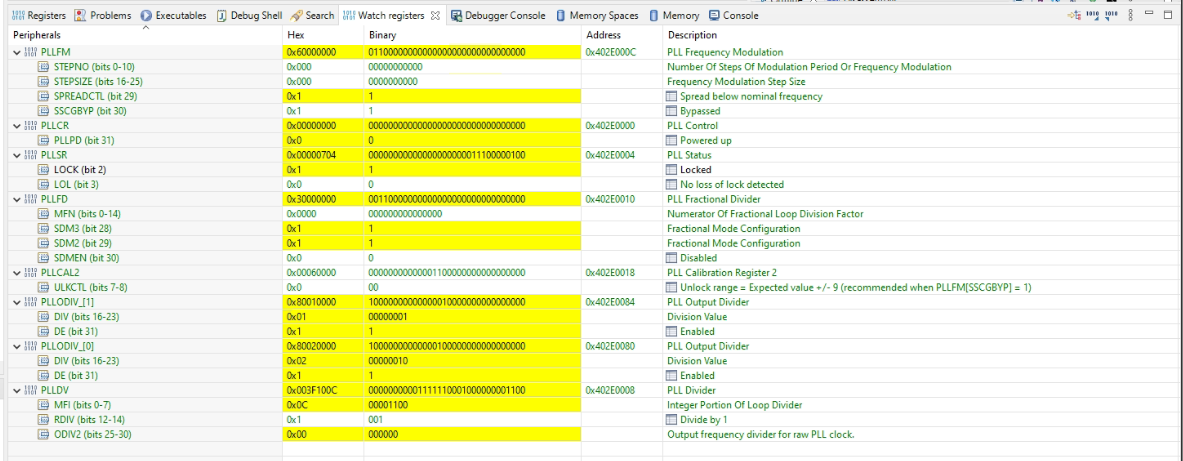
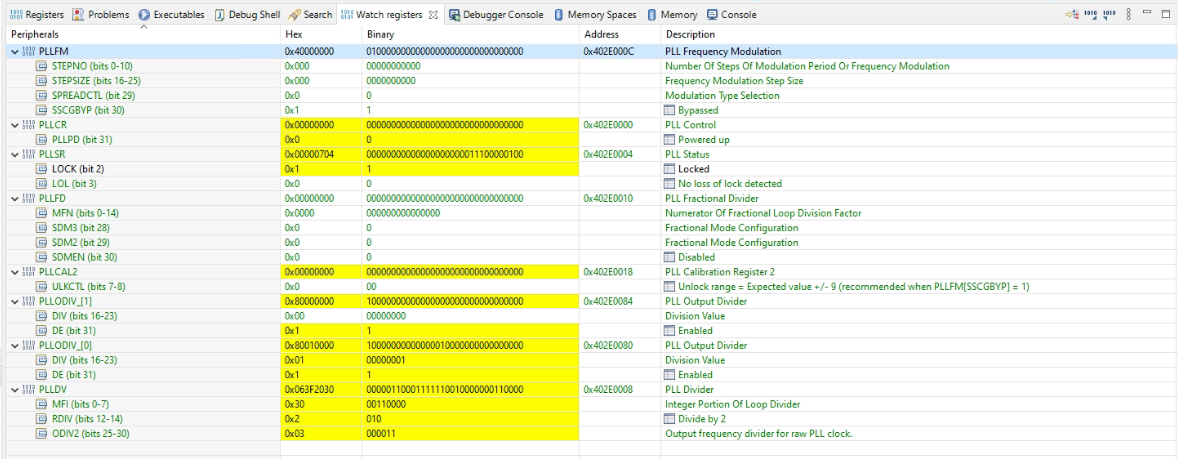
Thank you! I have enabled this setting, but the WRR instruction is still not sent correctly. Could this be caused by a misconfiguration of the PLL register?
I have compared the values of the PLL register when using sys_init (2_PLL_reg_sys_init.png) to the ones of the PLL register after using MCU Init (3_PLL_reg_mcu_init.png) and I have noticed differences for several PLL register fields (1_PLL_reg_values_comparison.png) .
The most notable are the down spread modulation (PLLFM->SPREADCTL) and the PLL Calibration Register 2 (PLLCAL2). I have checked the MCU manual (RTD_MCU_UM.pdf) and I see that PLLFM->SPREADCTL is only mentioned in a Tresos configuration (chapter 4.270 Parameter McuPllFmSpreadctl).
Is there any way I could also modify it with the classic Design Studio .mex approach?
Thank you,
Beatrice
Hi @maria_beatrice_balaceanu ,
For PLLFM->SPREADCTL you can select it as below:

For PLL Calibration Register 2 (PLLCAL2):

Best regards,
Nhi
Hi,
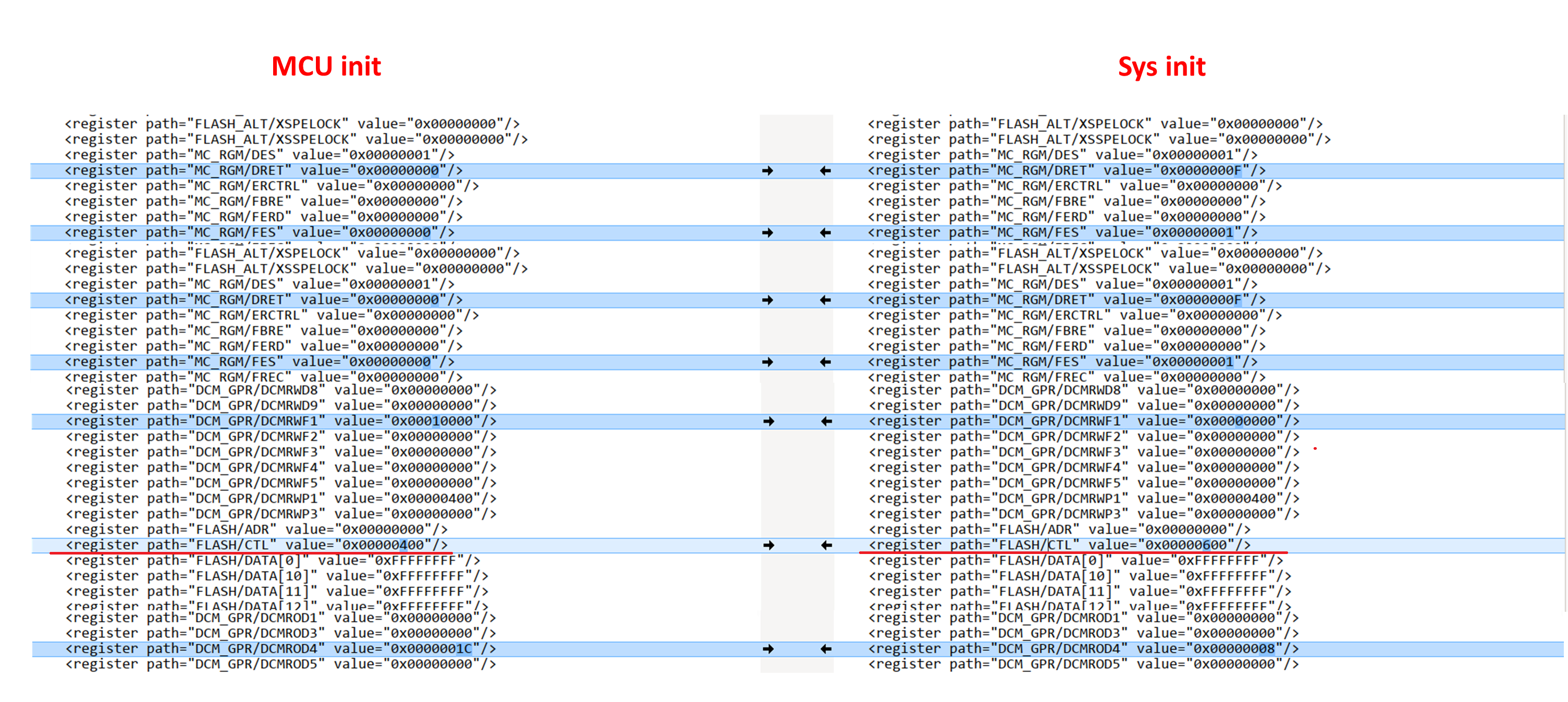
Thank you! I have also tried to modify the PLL and FXOSC registers from the MCU configuration, but the WRR instruction is still not sent correctly. I am attaching the project which I have tested to this message. I have also checked other registers and I see that the Wait States field of the FLASH/CTL register differs (1_RegistersComp.png), but I am not sure if this might impact anything. The other fields of the FLASH, FLASH_ALT, PFLASH, QUADSPI and CONFIGURATION_GPR are the same. Did you get a chance to check with your board?
Kind regards,
Beatrice
Hi, @Nhi_Nguyen,
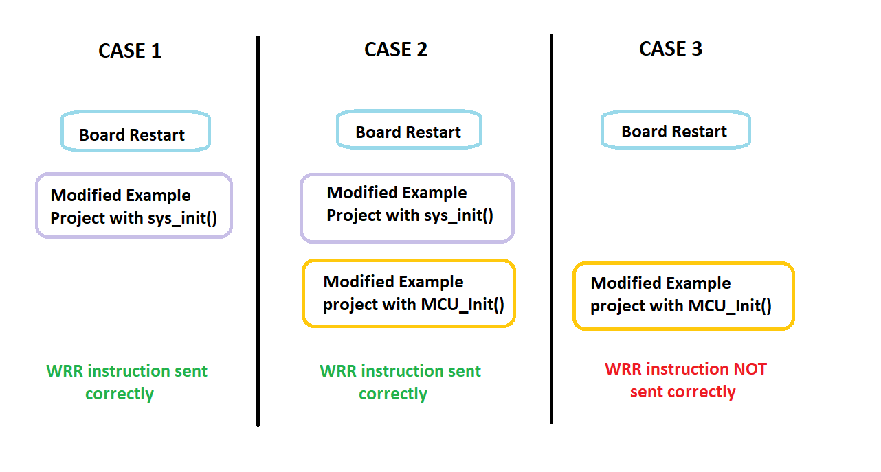
While testing, I have noticed another behavior of the QSPI module which might help. I have noticed that, if I restart the board by turning the power supply off and then back on, run the modified example with sys_init() and then run the same modified example with MCU_Init(), I get the correct WRR instruction sent (CASE 2 from 1_board_restart_behavior.png). If I restart the board and run the same modified example with MCU_Init(), the WRR instruction is no longer sent correctly (CASE 3 from 1_board_restart_behavior.png). Do you think there might be another setting/register (besides the QSPI, FXOSC, FIRC and SIRC ones) which could impact the write register operation?
Also, please let me know if you find anything on your board.
Thank you,
Beatrice
Hi @maria_beatrice_balaceanu ,
Can you please contact me through team? My acc: nhi.nguyenthikieu@nxp.com
Best regards,
Nhi
Thank you for your support! After our discussion, it seems that the most probable cause is a bug in the generated MCU driver, namely MUX_10_DC_0. We have requested a hotfix for this.
Hi, @Nhi_Nguyen ,
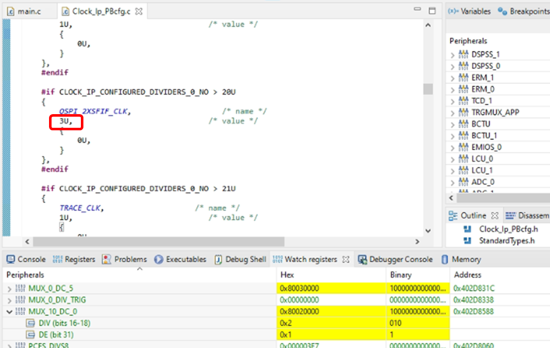
I have tried to modify manually the value which sets the MC_CGM/MUX_10_DC_0 to the same value as the one obtained with sys_init() (0x80020000) for PLL PHI1 at 240 MHz (1_DIV3.png), but the WRR instruction is still not sent correctly. I have also tried something similar with PLL PHI1 at 320 MHz, but still no luck.
Do you think there might be something else which corrupts this instruction?
Thank you,
Beatrice
Hi @maria_beatrice_balaceanu ,
I've just realized that a part of divider of MUX_10_DC done default by HW, so, we don't need to plus it to MUX_10_DC_DIV. So, it is not bug in driver. So, can you please cancel request to hotfix.
Just follow RM with option A+ memory
In DS configuration:
Best regards,
Nhi
Hi, @Nhi_Nguyen,
Thank you! I confirm that the WRR instruction is sent correctly with this configuration (RM 23.7.2.1 with Option A+). We have cancelled the hotfix request.
I have also tried to decrease the frequencies of the CORE_CLK and CM7_CORE_CLK clocks, while keeping the other frequencies the same as in RM 23.7.2.1 with Option A+, but then the WRR instruction is no longer sent correctly. Is RM 23.7.2.1 with Option A+ the only clock configuration for which the QSPI_IP_OP_TYPE_WRITE_REG operation sends the correct data?
Thank you!
Kind regards,
Beatrice
Hi @maria_beatrice_balaceanu ,
I don't think so. Because follow to RM for S32K396, have 2 clock options that support QuadSPI:

You can try to configure option B as below:


In configuration:


Best regards,
Nhi