- Forums
- Product Forums
- General Purpose MicrocontrollersGeneral Purpose Microcontrollers
- i.MX Forumsi.MX Forums
- QorIQ Processing PlatformsQorIQ Processing Platforms
- Identification and SecurityIdentification and Security
- Power ManagementPower Management
- Wireless ConnectivityWireless Connectivity
- RFID / NFCRFID / NFC
- Advanced AnalogAdvanced Analog
- MCX Microcontrollers
- S32G
- S32K
- S32V
- MPC5xxx
- Other NXP Products
- S12 / MagniV Microcontrollers
- Powertrain and Electrification Analog Drivers
- Sensors
- Vybrid Processors
- Digital Signal Controllers
- 8-bit Microcontrollers
- ColdFire/68K Microcontrollers and Processors
- PowerQUICC Processors
- OSBDM and TBDML
- S32M
- S32Z/E
-
- Solution Forums
- Software Forums
- MCUXpresso Software and ToolsMCUXpresso Software and Tools
- CodeWarriorCodeWarrior
- MQX Software SolutionsMQX Software Solutions
- Model-Based Design Toolbox (MBDT)Model-Based Design Toolbox (MBDT)
- FreeMASTER
- eIQ Machine Learning Software
- Embedded Software and Tools Clinic
- S32 SDK
- S32 Design Studio
- GUI Guider
- Zephyr Project
- Voice Technology
- Application Software Packs
- Secure Provisioning SDK (SPSDK)
- Processor Expert Software
- Generative AI & LLMs
-
- Topics
- Mobile Robotics - Drones and RoversMobile Robotics - Drones and Rovers
- NXP Training ContentNXP Training Content
- University ProgramsUniversity Programs
- Rapid IoT
- NXP Designs
- SafeAssure-Community
- OSS Security & Maintenance
- Using Our Community
-
- Cloud Lab Forums
-
- Knowledge Bases
- ARM Microcontrollers
- i.MX Processors
- Identification and Security
- Model-Based Design Toolbox (MBDT)
- QorIQ Processing Platforms
- S32 Automotive Processing Platform
- Wireless Connectivity
- CodeWarrior
- MCUXpresso Suite of Software and Tools
- MQX Software Solutions
- RFID / NFC
- Advanced Analog
-
- NXP Tech Blogs
- Home
- :
- Model-Based Design Toolbox (MBDT)
- :
- NXP Model-Based Design Tools Knowledge Base
- :
- Controlling LED intensity with ADC and PWM
Controlling LED intensity with ADC and PWM
- Subscribe to RSS Feed
- Mark as New
- Mark as Read
- Bookmark
- Subscribe
- Printer Friendly Page
- Report Inappropriate Content
Controlling LED intensity with ADC and PWM
Controlling LED intensity with ADC and PWM
1. Introduction
The purpose of this article is to illustrate how to configure and use the ADC and PWM peripherals of the MR-CANHUBK3 Evaluation board.
We will demonstrate how to develop an application which uses the on-board potentiometer to control the PWM duty cycle for the RED LED on the target. For more details on MR-CANHUBK344 and how to do the initial setup (Simulink® environment, J-Link debugger, etc.) please refer to Interacting with Digital Inputs/Outputs on MR-CANHUBK344 article.
2. ADC Configuration
2.1 Hardware Connections
The MR-CANHUBK344 evaluation board has multiple ADC channels that can be routed on various pins in complex applications. Our focus will be on the ADC channel corresponding to the potentiometer.
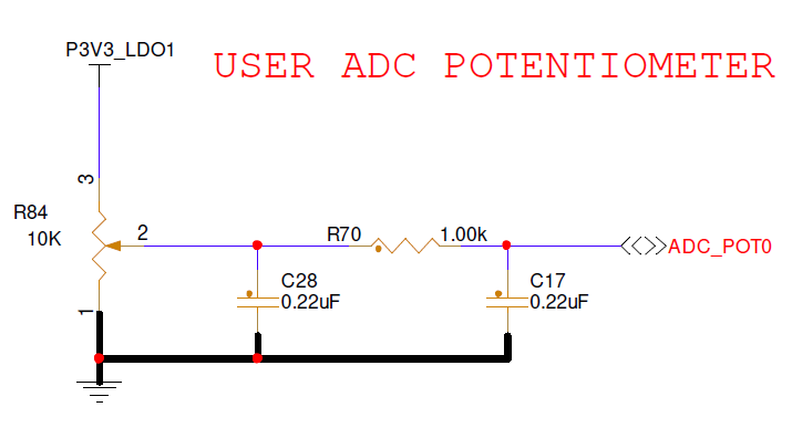
The potentiometer present on the board (R84) is a 10K trimmer potentiometer connected between 3V3 and GND and is connected to the net named ADC_POT0. This is further routed via pin 11 – PTE13/ADC1_S19.
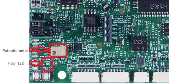
- Potentiometer and LED1 placement on the EVB:
Potentiometer schematic:
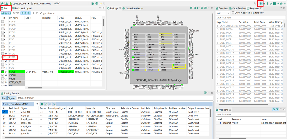
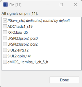
ADC_POT0 pin and its different routing options, with the correct one highlighted can be seen below:
The configuration of Adc component will be done in S32 Configuration Tools, but the same behavior can be achieved using EB Tresos.
2.2 Pins Configuration
Firstly, we need to specify the configuration options for the pin itself. This is done in the Pins menu of the S32 Configuration Tools, as follows:
1.We search for the PTE13 pin and check if it is already configured.
In this case it is not routed to any functionality, but, if it was routed to anything but ADC, we need to perform the same steps:
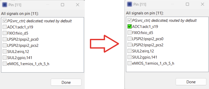
1.Click on the checkbox near the pin name:
2. Select ADC1:adc1_s19 from the pop-up window:
3.Provide a label and identifier for the newly mapped pin
In this example, the Label and Identifier are set to ADC_POT0
After the pin is configured, we move to the Routing Details menu:

- Direction to be configured as Input
- Input Buffer Enable to be configured as Enabled and update them accordingly if they aren’t.
2.3 Component Configuration
With the pins properly configured, we can move on to configure the Adc peripheral. We open the Adc component and begin by navigating to the AdcConfigSet tab where several steps need to be performed. In the AdcHwUnit menu, we first need to define a HW Unit for the ADC. If no HW unit is defined, a new one can be created by clicking the "+" button. We can modify the default configuration delivered with the toolbox and automatically assigned by MBDT in the new Simulink model or we can configure a new one. With the ADC peripheral instance defined, the first steps are to:
Name our HW unit. In this example it is named AdcHwUnit_0.
Select the ADC hardware of our unit. As we already know from the schematics, the potentiometer uses channel S19 of the ADC1, so we choose ADC1 for this configuration option.
The logical Unit ID is used to enumerate multiple HW units if present. Since for this example we only have one, we put the value 0 here.
For the transfer type we can choose between either Interrupt or DMA. For this example, we choose to use interrupts.
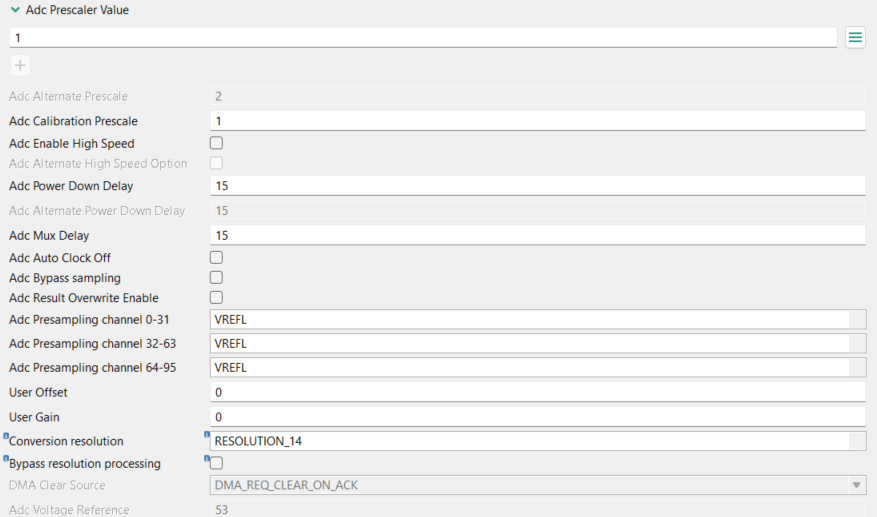
From the options presented below, most of them are not relevant for this example and can be kept with their defaults value.
An important setting is the conversion resolution. For this example, we chose the maximum resolution of 14, which corresponds to a maximum value of 2^14 (16384).
We can now move to the Channel definition inside the HW unit. If no channels are present, we can add a new one the same as before, by clicking the "+" button.
With a channel defined, the following configuration options need to be performed:
We need to specify the name of the ADC channel. For this example, we use ADC_POT_0. Note: This will be relevant when defining ADC groups. An ADC group is composed of multiple ADC channels.
Logical channel ID is 0 for this example since this is the only channel configured.
For the Physical Channel Name, we choose S19_ChanNum43 because we know we are on the S19 channel of the ADC. By looking in the S32Kxx Reference Manual we see that channel number 43 is mapped to ADC1_S19.
Physical Channel Id is just a mirror of the channel number from point 3.
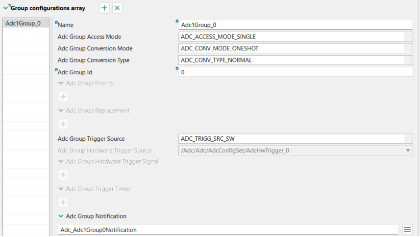
With both HW Unit and Channel in place, we need to define an Adc Group. Adc Groups are used to oversee conversion for the channels assigned to them. For this example, our group will only have one channel assigned, the ADC_POT_0.
In the Group configurations array menu, we click the "+" button to add our group.
We name our group. For this example, our group will be named Adc1Group_0.
Group access mode should be SINGLE.
Conversion Mode should be ONESHOT. When Conversion Mode is set to Oneshot, the ADC unit performs a single conversion and then waits to be triggered again.
Conversion Type should be NORMAL. Here we can choose between NORMAL and INJECTED conversion types; an injected conversion can be performed on top of a regular conversion, based on some external trigger(sensor, timer etc.). For this application we don’t need this feature.
Group ID is 0 since it is the only group configured.
Group Trigger source is SW
Group Notification function is Adc_Adc1Group0Notification . This is the callback function of the ADC group. The function pointer is called each time the group conversion is finished.
Note: underlined values at steps 1 and 7 are highlighted because they will be visible in Simulink blocks when we create our model.
We can configure several options for conversion as well. In this example we have HW average enabled, using 4 samples. This is done in order to mitigate noise that may occur on the readings without delaying too much the final results.
In the AdcGroupDefinition menu, we have to add our channel, as configured in the previous steps.
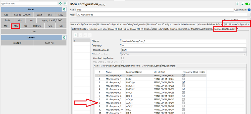
2.4 Clocks Configuration (MCU)
For the ADC to work properly, it needs to have its peripheral clock enabled. This is done inside the Mcu Peripheral, under McuModuleConfiguration tab -> McuModeSettingConf:
Important note here:
Since ADC_POT0(PTE13) is configured by default as VRC_CTRL,
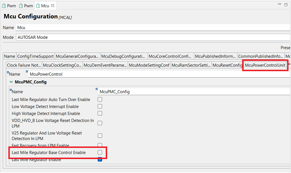
which is a PMC voltage regulator output that uses a BJT (Bipolar Junction Transistor) to generate a 1.5V supply, we need to disable this feature from Mcu configuration, otherwise we will not get accurate readings on the ADC pin.
This is done in the Mcu component, McuModuleConfiguration tab, McuPowerControlUnit menu, by disabling Last Mile Regulator Base Control Enable option:
2.5 Interrupts Configuration (Platform)
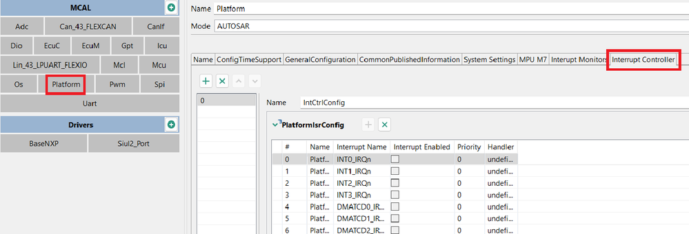
Since we opted to use the ADC in Interrupt Mode, we need to perform the correct configuration options inside Platform MCAL component.
The corresponding Interrupt Vector needs to be enabled, a priority must be given to it, and the correct handler function has to be specified from the RTD implementation.
All these options are configured inside Platform peripheral -> Interrupt Controller tab:
As it can be observed, the Interrupt Vector for ADC1 is enabled, has a priority of 5 and its handler function is Adc_Sar_1_Isr.
Finally, we save our configuration, we use the Update Code button and move to the model creation part of our example.
3. ADC Model Overview
With the configuration in place, the usage of S32 Configuration Tools (S32CT) is finished and we can implement our application in Simulink. In the following sections, we will go through the steps of creating a model that reads the potentiometer voltage and displays its value, converted into digital values, in FreeMASTER. More details FreeMASTER setup can be found in article 2.
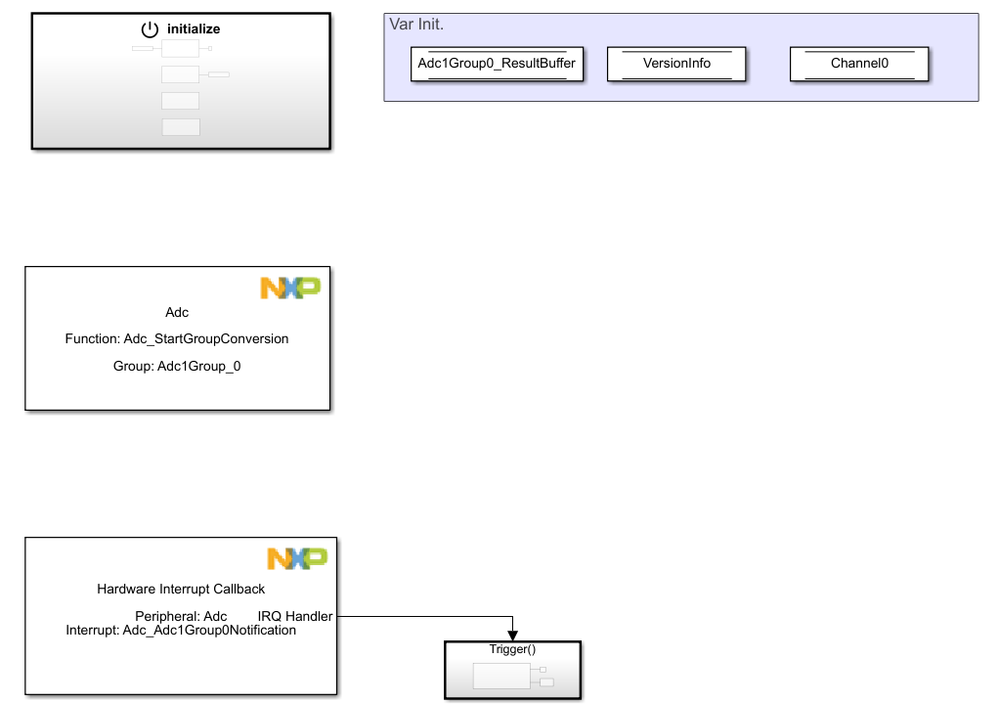
Model overview:
Going from top to bottom we have:
- 3 data store variables: the ADC VersionInfo, Adc1Group0_ResultBuffer, and Channel0.
- The initialize block
- The FreeMASTER config block
- The Start Group Conversion block
- The HW Interrupt Callback block, which triggers:
- The ADC Read Group block
All the ADC blocks can be found inside the MBDT:
The functionality is further detailed below:
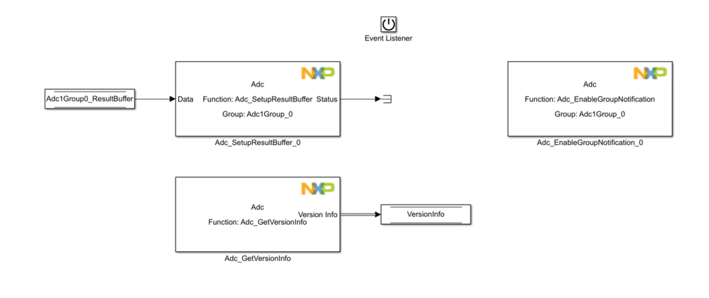
In the initialization block we prepare the SW for the ADC conversion by assigning the result buffer variable for our ADC group and by enabling the Group Notification.
Note: To be observed that the ADC Group used in both ADC blocks is exactly the same as the one underlined in 2.3 configuration chapter.
With the initialization done, the ADC group conversion can be started. This is performed periodically in the model’s step() function.
When the group conversion is finished, the group notification callback signals back to us that we can read the ADC value, and this is done into the subsystem triggered by the Hardware Interrupt block:

As it was observed in Sending data via UART and monitoring signals with FreeMASTER, FreeMASTER can be used to observe the evolution of a certain variable over time. We can use this feature to display the ADC readings stored on Channel0 on an oscilloscope.
We check if the values shown match our expectations when the Potentiometer is rotated. As it can be observed in the picture below, the values go from 0, up to 16384, and then back down to 0, as the potentiometer is rotated clockwise and then counterclockwise. This fully matches our expectations and validates that both the configuration and the Simulink application are implemented correctly.
4. PWM Configuration
4.1 Hardware Connections
The MR-CANHUBK344 is suited for various Pulse Width Modulation applications. The main PWM output port of the board is P8A, which in conjunction with P8B can be used to control and read feedback from common servomotors.
In this example , we are controlling the intensity of the RGB LED via PWM, based on the ADC readings from the potentiometer.
Note: The PWM control of the RGB LED is possible because each one of the 3 colored LEDs can also be routed via an eMIOS channel:
It is important to mention that we chose to generate our PWM signals using the Enhanced Modular IO Subsystem (eMIOS). eMIOS provides us independent channels, UCs (unified channels) that we can configure to generate or measure time events for different functions in different chip applications.
eMIOS distributes these channels across a number of global and local counter buses. Each local bus is dedicated to a group of eight contiguous channels. Each channel can generate its own timebase, and each counter bus has its timebase provided by a dedicated channel.
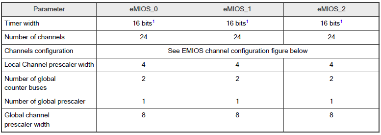
For the S32K344 MCU, we have 3 eMIOS instances available, each with the following configuration:
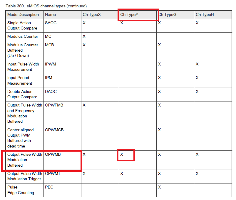
There are 4 different eMIOS channel types: X, Y, G and H. Each channel type supports a different subset of operation modes. More information can be found in “eMIOS channel types section of the S32K3xx MCU Family - Reference Manual :
It is important to be acquainted with the types of channels and their supported operation modes in order to be able to configure UCs properly, as some permutations may not be possible and configuration errors may occur.
The eMIOS is clocked by CORE_CLK, which has a frequency of 160 MHz. This is worth mentioning now, as it will become relevant when calculating the frequency of our PWM.
Important note: For this example, we choose to control the intensity of the Red LED ONLY, as the configuration steps for the other 2 LEDs would be similar.
Since we know that the Red LED is routed via CH19 of eMIOS_0, which is a type Y channel, we can choose to operate it via OPWMB Mode (Output Pulse Width Modulation Buffered). This mode comes with a fixed period for the PWM signal, variable(controllable) duty cycle and uses an external counter bus.
4.2 Pins Configuration
Firstly, we need to route the pin:
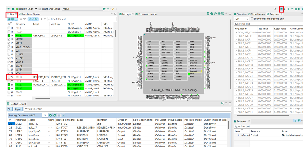
We look for the port and pin number of the red LED, and we observe it is part of Port E and has pin number 14:
As we did for the ADC pin, we look for PTE14 inside Pins tool , and we route it to eMIOS_0: emios_0_ch_19_y
When prompted, we select Output as direction for our pin. We provide a label and an identifier(RGBLED0_RED) for the pin.
In the Routing Details menu, we should have the following options configured:
Direction: Output; Output Inversion Select: Invert and OutputBuffer Enable: Enabled.
Note: If the configuration is done in EB Tresos and we add a new routing for the pin as PWM in the Port component, an error message will most likely appear. This can occur if the pin is already configured as a GPIO pin (DIO) inside Port component. To avoid this, the routing of the pin as a GPIO should be deleted.
4.3 Clocks Configuration (MCU)
As a prerequisite, we need to make sure that CORE_CLK is configured . This can be observed inside Mcu component -> McuModuleConfiguration tab -> McuClockSettingConfig menu -> McuClockReferencePoint submenu
Moreover, we need to make sure that the clock is enabled for the eMIOS instance we will be using:

4.4 MCL
As stated before, eMIOS can work using global or local buses. Different channels need to be assigned as timebase channels for the buses depending on the desired configuration:
- Global bus A: serves all UCs, uses CH23 as timebase
- Local bus B: serves UC0..UC7, uses CH0 as timebase
- Local bus C: serves UC8..UC15, uses CH8 as timebase
- Local bus
serves UC16..UC23, uses CH16 as timebase - Global bus F: serves all UCs, uses CH22 as timebase
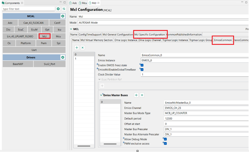
For example, we will use the global bus A and CH23 as master timer channel. This is configured inside Mcl component, as follows:
In the Mcl Specific Configuration tab, in EmiosCommon menu, we can add a new common eMIOS configuration, or we can modify an existing one to suit our needs.
We name our configuration
We select the eMIOS instance (eMIOS_0 in our case, since Red LED is routed via CH19 of eMIOS_0)
Clock Divider Value is used in frequency calculation and will be addressed separately. It has a range from 1 up to 256.
We need to define the time base channel for our master bus in its dedicated tab, as follows:
We name our time base channel
We select CH23, since we use Global Bus A
Default period and Master Bus Prescaler are used in frequency calculation. Default period can be any value from 0 up to 65534 and Master Bus Prescaler can be 1, 2, 3... up to 16.
PWM frequency calculation:
The PWM frequency needs to be decided upon based on the type of peripheral we want to actuate. For example, most servomotors operate at 50Hz, most BLDC motors support frequencies ranging from 5kHz up to 50kHz etc. This information needs to be known beforehand and configured according to the following formula:
A different way to think about this is by visualizing this formula having in mind the period of our PWM signal instead of its frequency:
Default Period is given in ticks, and the value of a tick is determined by the CORE_CLK frequency, divided by the 2 prescalers(Clock Divider Value and Master Bus Prescaler) and then inverted.
An undivided(both prescalers are 1) CORE_CLK tick has a value of 6.25 ns (1/160000000Hz).
Knowing the desired frequency for our application, we can determine its period. In order to have the same period, hence frequency, for the generated PWM signal, we need to adjust(or not, depending on the application) the values of the 2 prescalers in order to increase the CORE_CLK tick duration. The maximum value we can set for the Default Period is 65534; this value is then multiplied with the CORE_CLK tick duration after it is prescaled and the final result is the period of the PWM signal our application will generate.
Note: Without any prescaling, the maximum PWM period duration is roughly equal to 410 microseconds (6.25 ns * 65534), which corresponds to a frequency of ~2.4kHz. For applications that need slower frequencies, the CORE_CLK has to be prescaled. Ideally, the values for the prescalers and for the number of ticks should output an integer number for the period duration.
If we know our operating frequency f, we can adjust the 2 prescaler values and the default number of ticks to achieve it:
Example 1: If we know we need to actuate a servomotor with operating frequency of 50 Hz, we substitute in the formula the values we know (PWM_Frequency, CORE_CLK) and look for values of the prescalers and default number of ticks that do not exceed the configurable range. Note that multiple solutions are likely to be found and a suitable one needs to be chosen.
A possible solution for this specific frequency is Clock Divider Value = 256, Master Bus Prescaler = 1, Default Period = 12500. Another one is {128,4,6250}.
Example 2: If we know we need to actuate a BLDC with an operating frequency of 20kHz, a possible solution is {1,1,8000}. Another one is {2,2,2000}.
4.5 Component Configuration
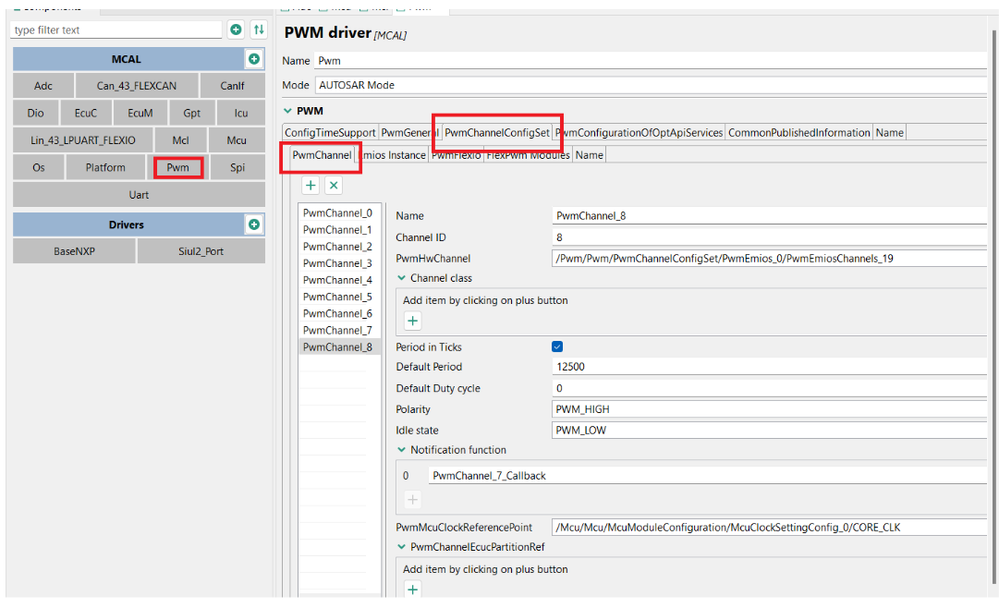
Inside the Pwm component, we need to perform 2 sets of configurations, one for the eMIOS channel and one for the PWM channel. Both can be performed in PwmChannelConfigSet tab.
4.5.1 eMIOS
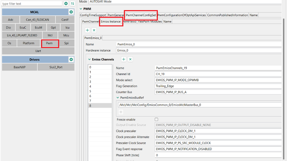
First of all, we need to add our eMIOS instance. This is done by clicking the "+" button at the top of the window. We need to make sure the proper hardware instance is selected, in our case, eMIOS_0.
With that in place, we can move to the configuration of the channels. If no channels are configured, a new one can be added using the "+" button. In our example, several channels are already configured, but our focus is on the 8th channel. With it selected, we set its name, we select the Channel ID to address 19th eMIOSchannel, select the desired operating mode(OPWMB), choose Bus A as a counter bus. For the PwmEmiosBusRef, we use the one previously configured at step 4.4.
We keep the prescalers at DIV_1 and we choose not to phase shift our signal, since it is not needed for our application.
4.5.2 Pwm Channel
With the eMIOS channel configured, we can move to the PWM channel configuration.
We add our channel, we give it a relevant name and assign it a channel ID. The Channel ID identifies the position of the channel in the configured list of channels.
For the PwmHwChannel option, we select the eMIOS channel configured at the previous step.
Default Period should have the same value as the one we defined for the Master Bus inside Mcl component, otherwise we will receive an error message.
Default Duty cycle represents the duty cycle forwarded to the LED at initialization. We keep it at 0 for our example.
At the PwmMcuClockReferencePoint option, we select CORE_CLK, as defined in the Mcu component.
Note: For this example, the use of interrupts was not needed. However, if interrupts have to be used, proper configuration settings must be done inside Platform component:

This concludes the configuration part of the PWM channel needed for our example and we can move on with the Simulink model.
5. PWM Model Overview
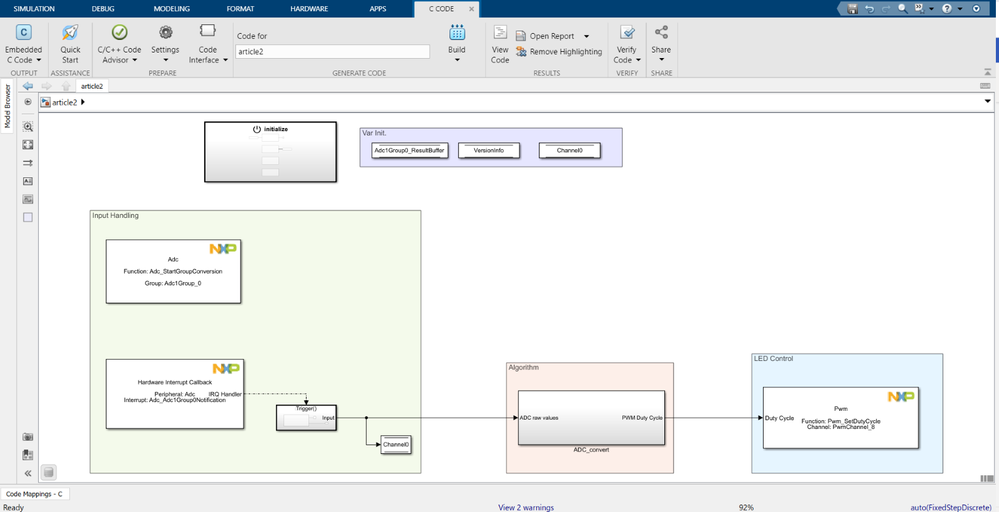
In order to implement this application, we will extend the ADC model created at step 3. Since we want to control the intensity of the LED based on the readings from the potentiometer, we will use the ADC converted potentiometer value as an input for the PWM channel.
Our application is structured into 4 parts:
- Initialization part
- Input Handling
- Algorithm
- Output Setting
The Initialization and Input handling sections of our application are similar to the ones present in the model created at step 3 of this article, the only exception being that the ADC reading is not only stored inside Channel0 variable, but it is also fed into the algorithm.
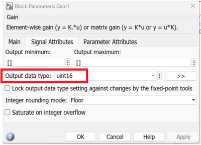
Our application’s algorithm’s goal is to convert the raw values provided by the ADC into values that are accepted by the PWM block. Since our input values need to be scaled up with a factor of 2, we need to apply the Gain block from Simulink.
We need to consider that the Pwm Block expects an argument of uint16 data type, so we need to make sure that the gain applied is of that type:
The output of our application is represented by the LED intensity (i.e. the duty cycle). One important mention here is that the duty cycle is not expressed as a percentage, but as a value from 0 to 32768 (0 -> 0% duty; 16384 -> 50% duty; 32768 -> 100% duty).
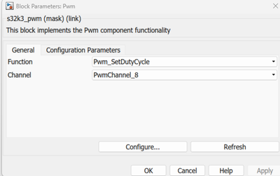
For the output control, we need to use a Pwm block from the MBDT:
We drag and drop the Pwm block into our canvas, we select the desired function (Pwm_SetDutyCycle) in our case, and also the Pwm channel we want to control(we choose the PWM channel configured at 4.5.2 step, in our case PwmChannel_8; all the channels selectable from the drop-down list are the ones previously configured in S32CT) :
We apply the algorithm to the input value and feed the result into the PWM block:
Below, a video showcasing the functionality can be found
In the first part of the video, the potentiometer is rotated clockwise and the duty cycle of the LED gradually reaches 100%, then, in the second half of the video, the potentiometer is rotated in the opposite direction and the LED can be observed dimming down until it turns back off completely.
Note: The status LEDs were covered with black tape so that the Red LED's intensity can be seen more clearly
6. Conclusion
ADC and PWM are 2 peripherals with a large applicability domain and they are frequently used in embedded applications. The goal of the article was to extend the general knowledge about those 2 peripherals and apply it on a hands-on example using MR-CANHUBK344 Evaluation board. The LED intensity dimming example illustrated in this article covers the configuration part of both peripherals, the development of an algorithm that handles input values and feeds them to the output and, together with the previous articles, helps us understand better the integration process of embedded applications using Model-Based Design Toolbox.
Instructions on how to run the attached model:
- Download and extract the archive’s contents;
- Copy both the .mdl and .mex file to the location where you wish to set up the project;
Note: for the model to work properly, please place the .mex file next to the model. - Open the .mdl file and make sure that MATLAB’s Current Folder points to the folder that contains the model;
- Click on the Hardware tab and then press the “Build, Deploy & Start” button.
Simulink is a registered trademark of The MathWorks, Inc. See mathworks.com/trademarks for a list of additional trademarks.
- Mark as Read
- Mark as New
- Bookmark
- Permalink
- Report Inappropriate Content
Hi,
I want to use EXT_ADC1 on PTE0 to drive the LED intensity based on Input voltage on the PIN (6 of P8B).
I have configured the PTE0, however, I observe that the ADC read value is stable only when the PIN is set to ground or when the pin is set to VCC. For all other variations in the voltage the ADC read value keeps on oscillating.
Oscilloscope when Pin is connected to Ground
Oscilloscope when Pin is connected to VCC
Oscilloscope when Pin is connected to 1V
How do I read the voltage steadily on the PIN ? Thanks
-Ankit
- Mark as Read
- Mark as New
- Bookmark
- Permalink
- Report Inappropriate Content
Hello Ankit!
I modified the example provided in the article to read the voltage on EXT_ADC1 Pin instead of POT0 and it seems everything is working as expected.
Apart from routing the PTE0 Pin, it is also required to modify the ADC Channel from Adc Peripheral(from ADC1_S19 ChanNum43 to ADC1_P2 ChanNum2).
I am attaching the updated configuration file, so that you are able to make a comparison and see what is missing.
Note: With the updated configuration and the rest of the example unchanged, the LED intensity should vary based on the voltage applied to P8B Pin6 instead of the Potentiometer readings.
I hope this explanation was helpful.
- Mark as Read
- Mark as New
- Bookmark
- Permalink
- Report Inappropriate Content
Hi,
Such a good article! I learned a lot.
However, rather than PWM output, PWM input seems more challenging since there are no eMIOS or PWM input models in this toolbox. I wonder if can give some explanations or demos about how to use IPM (Input Period Measurement) with custom code, I really need these functions in developing a motor-control program.
Thanks!
- Mark as Read
- Mark as New
- Bookmark
- Permalink
- Report Inappropriate Content
Thanks for the article!!
If there are multiple channels within a group, how would you read each individual channels? The output of the Adc_ReadGroup is a single uint16, regardless of how many channels are configured within the group. Would I need to create a new group for each channel?
- Mark as Read
- Mark as New
- Bookmark
- Permalink
- Report Inappropriate Content
ı have a s32g339 card and i want to run the ADC by my card and ı dont have any examples can you share wtih me some steps to run my adc ı will use potentialmeter
