- NXP Forums
- Product Forums
- General Purpose MicrocontrollersGeneral Purpose Microcontrollers
- i.MX Forumsi.MX Forums
- QorIQ Processing PlatformsQorIQ Processing Platforms
- Identification and SecurityIdentification and Security
- Power ManagementPower Management
- MCX Microcontrollers
- S32G
- S32K
- S32V
- MPC5xxx
- Other NXP Products
- Wireless Connectivity
- S12 / MagniV Microcontrollers
- Powertrain and Electrification Analog Drivers
- Sensors
- Vybrid Processors
- Digital Signal Controllers
- 8-bit Microcontrollers
- ColdFire/68K Microcontrollers and Processors
- PowerQUICC Processors
- OSBDM and TBDML
-
- Solution Forums
- Software Forums
- MCUXpresso Software and ToolsMCUXpresso Software and Tools
- CodeWarriorCodeWarrior
- MQX Software SolutionsMQX Software Solutions
- Model-Based Design Toolbox (MBDT)Model-Based Design Toolbox (MBDT)
- FreeMASTER
- eIQ Machine Learning Software
- Embedded Software and Tools Clinic
- S32 SDK
- S32 Design Studio
- GUI Guider
- Zephyr Project
- Voice Technology
- Application Software Packs
- Secure Provisioning SDK (SPSDK)
- Processor Expert Software
-
- Topics
- Mobile Robotics - Drones and RoversMobile Robotics - Drones and Rovers
- NXP Training ContentNXP Training Content
- University ProgramsUniversity Programs
- Rapid IoT
- NXP Designs
- SafeAssure-Community
- OSS Security & Maintenance
- Using Our Community
-
- Cloud Lab Forums
-
TVDD filtering for NFC
09-12-2022
08:16 AM
548 次查看
Hello, I am making a design with the CLEV663 NFC controller. I notice a slight discrepancy between the chip's datasheet and the Development Board schematic, specifically for the TVDD (transmitter voltage supply pins).
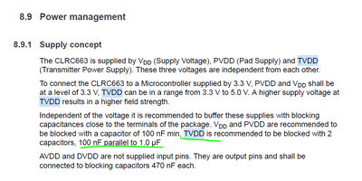
The datasheet for CLRC663 recommends 2 blocking caps, 100nF in parallel with 1.0uF. See below.
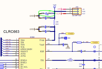
The development board schematic uses a 100nF and a 100uF (polarized, tantalum listed in BOM as C300 too).
1.0uF and 100uF are a big difference. Is there any technical justification for using the larger cap found in the schematic and disregarding the datasheet material?
Any other insight into the added inductor and caps connected to the TVDD pin (L300, C302, C303)?
Thanks!
0 回复数

