- Forums
- Product Forums
- General Purpose MicrocontrollersGeneral Purpose Microcontrollers
- i.MX Forumsi.MX Forums
- QorIQ Processing PlatformsQorIQ Processing Platforms
- Identification and SecurityIdentification and Security
- Power ManagementPower Management
- Wireless ConnectivityWireless Connectivity
- RFID / NFCRFID / NFC
- Advanced AnalogAdvanced Analog
- MCX Microcontrollers
- S32G
- S32K
- S32V
- MPC5xxx
- Other NXP Products
- S12 / MagniV Microcontrollers
- Powertrain and Electrification Analog Drivers
- Sensors
- Vybrid Processors
- Digital Signal Controllers
- 8-bit Microcontrollers
- ColdFire/68K Microcontrollers and Processors
- PowerQUICC Processors
- OSBDM and TBDML
- S32M
- S32Z/E
-
- Solution Forums
- Software Forums
- MCUXpresso Software and ToolsMCUXpresso Software and Tools
- CodeWarriorCodeWarrior
- MQX Software SolutionsMQX Software Solutions
- Model-Based Design Toolbox (MBDT)Model-Based Design Toolbox (MBDT)
- FreeMASTER
- eIQ Machine Learning Software
- Embedded Software and Tools Clinic
- S32 SDK
- S32 Design Studio
- GUI Guider
- Zephyr Project
- Voice Technology
- Application Software Packs
- Secure Provisioning SDK (SPSDK)
- Processor Expert Software
- Generative AI & LLMs
-
- Topics
- Mobile Robotics - Drones and RoversMobile Robotics - Drones and Rovers
- NXP Training ContentNXP Training Content
- University ProgramsUniversity Programs
- Rapid IoT
- NXP Designs
- SafeAssure-Community
- OSS Security & Maintenance
- Using Our Community
-
- Cloud Lab Forums
-
- Knowledge Bases
- ARM Microcontrollers
- i.MX Processors
- Identification and Security
- Model-Based Design Toolbox (MBDT)
- QorIQ Processing Platforms
- S32 Automotive Processing Platform
- Wireless Connectivity
- CodeWarrior
- MCUXpresso Suite of Software and Tools
- MQX Software Solutions
- RFID / NFC
- Advanced Analog
-
- NXP Tech Blogs
- Home
- :
- 汎用マイクロコントローラ
- :
- LPCマイクロコントローラ
- :
- External SRAM LPC54628
External SRAM LPC54628
- RSS フィードを購読する
- トピックを新着としてマーク
- トピックを既読としてマーク
- このトピックを現在のユーザーにフロートします
- ブックマーク
- 購読
- ミュート
- 印刷用ページ
External SRAM LPC54628
- 新着としてマーク
- ブックマーク
- 購読
- ミュート
- RSS フィードを購読する
- ハイライト
- 印刷
- 不適切なコンテンツを報告
Hi,
I'm trying to interface 16-bit external DPRAM (Dual Port RAM) 70V261 with LPC54628 using its EMC peripheral.
Query 1:
If data is read from the DPRAM immediately after a write, then all read operations are successful. However, if data is first written to DPRAM, some delay is inserted and then read operation is performed, most of the read operations fail. However, there is a fixed pattern between the value that is written to the DPRAM and the incorrect value that is read back. Basically,
Readback value = (original value that was written << 16U) + 0x0100.
| Value that was written | Readback value | EMC location (address, HEX) | Diff between written and read value | Diff in HEX |
| 0 | 256 | x80000000 | 256 | x0100 |
| 1 | 513 | x80000001 | 512 | x0200 |
| 2 | 770 | x80000002 | 768 | x0300 |
| 3 | 1027 | x80000003 | 1024 | x0400 |
void DPRAM_full_emc_test_code(void){
	DP_read_after_write(0x80000000, 16384U);
	delay_1ms(100U);
	DP_only_read(0x80000000, 16384U);

	while(1){
		__NOP();
	}
}

void DP_read_after_write(uint32_t DPRAM_base_add, uint16_t len){
	for (uint16_t p=0; p< len; p++){
		*(uint16_t *)(DPRAM_base_add + p) = p;
		temp16_1 = 0;
		temp16_1 = *(uint16_t *)(DPRAM_base_add + p);

		if (temp16_1 != p){
			PRINTF("Mismatch, p=%d, rb_val: d%d, Add: x%x \r\n",  p, temp16_1, (DPRAM_base_add + p));
		}
		else {
		}
	}
	PRINTF("W&R complete\r\n");
}

void DP_only_read(uint32_t DPRAM_base_add, uint16_t len){
	for (uint16_t p=0; p< len; p++){
		temp16_1 = 0;
		temp16_1 = *(uint16_t *)(DPRAM_base_add + p);

		if (temp16_1 != p){
			PRINTF("Mismatch, %d, %d, x%x \r\n",  p, temp16_1, (DPRAM_base_add + p));
		}
		else {
			PRINTF("Read Ok\r\n");
		}
	}
}
As you can see, the lower 8 bits are always zeroes. Any idea what I could be doing wrong?
Query 2:
Can you suggest what could causing the following runtime error? I had to comment out a certain section of the code in 'EMC_StaticMemInit_custom' that deals with 'ExtendedWait' to avoid this runtime error. Now I am not sure whether the readback value mismatch in Query-1 has something to do with 'Ext Wait' code being commented out. Compiler is Keil.
*** assertion failed: staticConfig->specailConfig & kEMC_AsynchronosPageEnable, file C:\Users\Admin\AppData\Local\Arm\Packs\NXP\LPC54628_DFP\12.0.0\drivers\fsl_emc.c, line 374

SIGABRT: Abnormal termination
Code:
void DPRAM_Init_full_EMC(void){
	uint32_t emcFreq, emc_static_wait;
	emc_basic_config_t basicConfig;
	emc_static_chip_config_t staticchipconfig;
	emcFreq = CLOCK_GetFreq(kCLOCK_EMC);
	assert(emcFreq != 0);
	basicConfig.endian   = kEMC_LittleEndian;
	basicConfig.fbClksrc=kEMC_IntloopbackEmcclk;
	basicConfig.emcClkDiv = 1;
	EMC_Init_custom(EMC, &basicConfig);
	staticchipconfig.chipIndex = 0;
	staticchipconfig.memWidth = kEMC_16BitWidth;
	staticchipconfig.specailConfig = kEMC_ExtWaitEnable ;
	staticchipconfig.tWaitOutEn_Ns = 5U;
	staticchipconfig.tWaitReadNoPage_Ns = 100U
	staticchipconfig.tWaitReadPage_Ns = 5U;
	staticchipconfig.tWaitTurn_Ns = 5U;
	staticchipconfig.tWaitWriteEn_Ns = 5U;
	staticchipconfig.tWaitWrite_Ns = 20U;
//	emc_static_wait =  25U;

	EMC_StaticMemInit_custom(EMC, &emc_static_wait, &staticchipconfig, 1);
	EMC_Enable(EMC, true);
}


void EMC_StaticMemInit_custom(EMC_Type *base, uint32_t *extWait_Ns, emc_static_chip_config_t *config, uint32_t totalChips){
	assert(config);

	uint32_t count;
	emc_static_chip_config_t *staticConfig = config;

	// Commented out extended_wait configuration
	// If this is not commented out, then  'assertion failed: staticConfig->specailConfig & kEMC_AsynchronosPageEnable,' runtime error will occur.
	/*
	if (extWait_Ns){
		for (count = 0; (count < totalChips) && (staticConfig != NULL); count++){
			assert(staticConfig->specailConfig & kEMC_ExtWaitEnable);
		}

		base->STATICEXTENDEDWAIT = EMC_CalculateTimerCycles_custom(base, *extWait_Ns, 1);
		PRINTF("STATICEXTENDEDWAIT=%d\r\n", EMC_CalculateTimerCycles_custom(base, *extWait_Ns, 1));
		staticConfig++;
	}
	*/

	/* Initialize the static memory chip specific configure. */
	staticConfig = config;
	for (count = 0; (count < totalChips) && (staticConfig != NULL); count++){
		base->STATIC[staticConfig->chipIndex].STATICCONFIG =  (staticConfig->specailConfig | staticConfig->memWidth);

		base->STATIC[staticConfig->chipIndex].STATICCONFIG &= ~0x100;	// make EW bit 0 to disable Extended Wait
		base->STATIC[staticConfig->chipIndex].STATICCONFIG |= 0x80;	// make PB bit 1

		base->STATIC[staticConfig->chipIndex].STATICWAITWEN = EMC_CalculateTimerCycles_custom(base, staticConfig->tWaitWriteEn_Ns, 1);		//d'0'
//		PRINTF("STATICWAITWEN=%d\r\n", EMC_CalculateTimerCycles_custom(base, staticConfig->tWaitWriteEn_Ns, 1));

		base->STATIC[staticConfig->chipIndex].STATICWAITOEN = EMC_CalculateTimerCycles_custom(base, staticConfig->tWaitOutEn_Ns, 0);		//d'1'
//		PRINTF("STATICWAITOEN=%d\r\n", EMC_CalculateTimerCycles_custom(base, staticConfig->tWaitOutEn_Ns, 0));

		base->STATIC[staticConfig->chipIndex].STATICWAITRD = EMC_CalculateTimerCycles_custom(base, staticConfig->tWaitReadNoPage_Ns, 1);		//d'19'
//		PRINTF("STATICWAITRD=%d\r\n", EMC_CalculateTimerCycles_custom(base, staticConfig->tWaitReadNoPage_Ns, 1));

		base->STATIC[staticConfig->chipIndex].STATICWAITPAGE = EMC_CalculateTimerCycles_custom(base, staticConfig->tWaitReadPage_Ns, 1);		//d'0'
//		PRINTF("STATICWAITPAGE=%d\r\n", EMC_CalculateTimerCycles_custom(base, staticConfig->tWaitReadPage_Ns, 1));

		base->STATIC[staticConfig->chipIndex].STATICWAITWR = EMC_CalculateTimerCycles_custom(base, staticConfig->tWaitWrite_Ns, 2);		//d'0'
//		PRINTF("STATICWAITWR=%d\r\n", EMC_CalculateTimerCycles_custom(base, staticConfig->tWaitWrite_Ns, 2));

		base->STATIC[staticConfig->chipIndex].STATICWAITTURN = EMC_CalculateTimerCycles_custom(base, staticConfig->tWaitTurn_Ns, 1);		//d'0'
//		PRINTF("STATICWAITTURN=%d\r\n", EMC_CalculateTimerCycles_custom(base, staticConfig->tWaitTurn_Ns, 1));

		staticConfig++;
	}
}


static uint32_t EMC_CalculateTimerCycles_custom(EMC_Type *base, uint32_t timer_Ns, uint32_t plus){
	uint32_t cycles;
	cycles = CLOCK_GetEmcClkFreq() / EMC_HZ_ONEMHZ * timer_Ns;
	cycles = EMC_DIV_ROUND_UP(cycles, EMC_MILLISECS_ONESEC); /* Round up. */

	/* Decrese according to the plus. */
	if (cycles >= plus){
		cycles = cycles - plus;
	}
	else{
		cycles = 0;
	}
	return cycles;
}


void EMC_Init_custom(EMC_Type *base, emc_basic_config_t *config){
#if !(defined(FSL_SDK_DISABLE_DRIVER_CLOCK_CONTROL) && FSL_SDK_DISABLE_DRIVER_CLOCK_CONTROL)
    /* Enable the clock. */
    CLOCK_EnableClock((s_EMCClock[EMC_GetInstance_custom(base)]));
#endif /* FSL_SDK_DISABLE_DRIVER_CLOCK_CONTROL */

#if !(defined(FSL_FEATURE_EMC_HAS_NO_RESET) && FSL_FEATURE_EMC_HAS_NO_RESET)
    /* Reset the EMC module */
    RESET_PeripheralReset(s_emcResets[EMC_GetInstance_custom(base)]);
#endif

    /* Reset the EMC. */
    SYSCON->PRESETCTRL[2] |= SYSCON_PRESETCTRL_EMC_RESET_MASK;
    SYSCON->PRESETCTRL[2] &= ~SYSCON_PRESETCTRL_EMC_RESET_MASK;

    /* Set the EMC sytem configure. */
    SYSCON->EMCCLKDIV = SYSCON_EMCCLKDIV_DIV(config->emcClkDiv);
    SYSCON->EMCSYSCTRL = SYSCON_EMCSYSCTRL_EMCFBCLKINSEL(config->fbClkSrc);

	// Added next two lines to modify EMCSYSCTRL to make the code work
	SYSCON->EMCSYSCTRL &= ~0x01;	// make LSB bit0 = '0', so that addresses are shifted to match bus width to ensure 1:1 relation between address lines
	SYSCON->EMCSYSCTRL |= 0x04;		// make bit2 = 1 to disable burst mode

    /* Set the endian mode. */
    base->CONFIG = config->endian;
    /* Enable the EMC module with normal memory map mode and normal work mode. */
    base->CONTROL = EMC_CONTROL_E_MASK;
}


static uint32_t EMC_GetInstance_custom(EMC_Type *base){
	uint32_t instance;

	/* Find the instance index from base address mappings. */
	for (instance = 0; instance < ARRAY_SIZE(s_EMCBases); instance++){
		if (s_EMCBases[instance] == base){
			break;
		}
	}
	assert(instance < ARRAY_SIZE(s_EMCBases));
	return instance;
}
.
- 新着としてマーク
- ブックマーク
- 購読
- ミュート
- RSS フィードを購読する
- ハイライト
- 印刷
- 不適切なコンテンツを報告
Pressed reply button by mistake. Can't see DELETE POST option.
Please don't miss the reply I posted a few minutes ago.
- 新着としてマーク
- ブックマーク
- 購読
- ミュート
- RSS フィードを購読する
- ハイライト
- 印刷
- 不適切なコンテンツを報告
First of all, thanks to both of you for the response.
@frank_m Were you able to resolve the issue? If yes, can you please share how it was resolved?
I made the changes you suggested and the result is the same.
However, I configured the BLSN0 & 1 pins (Upper Byte & Lower Byte selection pins) as GPIO type and set it permanently to logic low since my DPRAM is 16-bit and my values are stored as 16-bit numbers. This improved the result substantially. Now all odd addresses are read back successfully while even addresses have the left_shift I described in the first post. I also tried to set the values for various delays manually by loading values into respective registers and printed the values to terminal, as can be seen from the code.
Configuration in brief:
16-bit width, little endian, core PLL frequency 96MHz, page mode disabled, active low chip select, byte lane state bit PB is high, extended wait disabled, buffer disabled.
Static memory addresses shifted to match data bus width (bit-0 of uC connected to bit-0 of DPRAM), burst disabled, EMC clock source is internal loop back from EMC_CLK output.
Output:
SYSCON->EMCSYSCTRL: 0x4
EMC->CONTROL: 0x1
EMC->STATUS: 0x5
EMC->CONFIG: 0x0
EMC->STATICEXTENDEDWAIT: 0x0
EMC->STATIC[0].STATICCONFIG: 0x81
EMC->STATIC[0].STATICWAITWEN: 0x0
EMC->STATIC[0].STATICWAITOEN: 0x0
EMC->STATIC[0].STATICWAITRD: 0x1
EMC->STATIC[0].STATICWAITPAGE: 0x0
EMC->STATIC[0].STATICWAITWR: 0x0
EMC->STATIC[0].STATICWAITTURN: 0x0

W&R complete
Mismatch, 0, 256, x80000000
Read Ok
Mismatch, 2, 768, x80000002
Read Ok
Mismatch, 4, 1280, x80000004
Read Ok
Mismatch, 6, 1792, x80000006
Read Ok
Mismatch, 8, 2304, x80000008
Read Ok
Mismatch, 10, 2816, x8000000a
Read Ok
Mismatch, 12, 3328, x8000000c
Read Ok
Mismatch, 14, 3840, x8000000e
Read Ok
Mismatch, 16, 4352, x80000010
Read Ok
Mismatch, 18, 4864, x80000012
Read Ok
Mismatch, 20, 5376, x80000014
Read Ok
Mismatch, 22, 5888, x80000016
Read Ok
Mismatch, 24, 6400, x80000018
Code:
void DPRAM_Config_pins_full_EMC(void){
	IOCON->PIO[0][EMC_A0_R] = // 18 ok
	IOCON->PIO[0][EMC_A1_R] = // 19 ok
	IOCON->PIO[0][EMC_A2_R] = // 20 ok
	IOCON->PIO[0][EMC_A3_R] = // 21 ok
	IOCON->PIO[1][EMC_A4_R] = // 5 ok
	IOCON->PIO[1][EMC_A5_R] = // 6 ok
	IOCON->PIO[1][EMC_A6_R] = // 7 ok
	IOCON->PIO[1][EMC_A7_R] =	// 8 ok
	IOCON->PIO[1][EMC_A8_R] = // 26 ok
	IOCON->PIO[1][EMC_A9_R] = // 27 ok
	IOCON->PIO[1][EMC_A10_R] = // 16 ok
	IOCON->PIO[1][EMC_A11_R] = // 23 ok
	IOCON->PIO[1][EMC_A12_R] = // 24 ok
	IOCON->PIO[1][EMC_A13_R]  	// 25 ok
	 = IOCON_PIO_FUNC6 | IOCON_PIO_MODE_INACT | IOCON_PIO_INV_DI | IOCON_PIO_DIGITAL_EN | IOCON_PIO_INPFILT_OFF | IOCON_PIO_SLEW_FAST | IOCON_PIO_OPENDRAIN_DI;

	IOCON->PIO[0][EMC_IO_0R] =	// 2 ok
	IOCON->PIO[0][EMC_IO_1R] =	// 3 ok
	IOCON->PIO[0][EMC_IO_2R] =	// 4 ok
	IOCON->PIO[0][EMC_IO_3R] =	// 5 ok
	IOCON->PIO[0][EMC_IO_4R] =	// 6 ok
	IOCON->PIO[0][EMC_IO_5R] =	// 7 ok
	IOCON->PIO[0][EMC_IO_6R] =	// 8 ok
	IOCON->PIO[0][EMC_IO_7R] = 	// 9 ok
	IOCON->PIO[1][EMC_IO_8R] =	// 19 ok
	IOCON->PIO[1][EMC_IO_9R] =	// 20 ok
	IOCON->PIO[1][EMC_IO_10R] =	// 21 ok
	IOCON->PIO[1][EMC_IO_11R] =	// 4 ok
	IOCON->PIO[1][EMC_IO_12R] =	// 28 ok
	IOCON->PIO[1][EMC_IO_13R] =	// 29 ok
	IOCON->PIO[1][EMC_IO_14R] =	// 30 ok
	IOCON->PIO[1][EMC_IO_15R] 	// 31 ok
	 = IOCON_PIO_FUNC6 | IOCON_PIO_MODE_INACT | IOCON_PIO_INV_DI | IOCON_PIO_DIGITAL_EN | IOCON_PIO_INPFILT_OFF | IOCON_PIO_SLEW_FAST | IOCON_PIO_OPENDRAIN_DI;

	IOCON->PIO[0][EMC_RW_R] 	//  0_15 is EMC_WEN	(Write Enable, active low)
	 = IOCON_PIO_FUNC6 | IOCON_PIO_MODE_INACT | IOCON_PIO_INV_DI | IOCON_PIO_DIGITAL_EN | IOCON_PIO_INPFILT_OFF | 	IOCON_PIO_OPENDRAIN_DI;

	IOCON->PIO[0][EMC_CE_R]  //OK. 0_16 is EMC_CSN[0]	(Chip select, active low)
	 = IOCON_PIO_FUNC6 | IOCON_PIO_MODE_INACT | IOCON_PIO_INV_DI | IOCON_PIO_DIGITAL_EN | IOCON_PIO_INPFILT_OFF | IOCON_PIO_OPENDRAIN_DI;

	IOCON->PIO[0][EMC_OE_R] //  0_17 is EMC_OEN  (Output Enable, active low)
	 = IOCON_PIO_FUNC6 | IOCON_PIO_MODE_INACT | IOCON_PIO_INV_DI | IOCON_PIO_DIGITAL_EN | IOCON_PIO_INPFILT_OFF | IOCON_PIO_OPENDRAIN_DI;

	IOCON->PIO[1][EMC_LB_R] 	//  1_17 is EMC_BLSN0(Byte Lane Select 0, active low)
	 = IOCON_PIO_FUNC0 | IOCON_PIO_MODE_INACT | IOCON_PIO_INV_DI | IOCON_PIO_DIGITAL_EN | IOCON_PIO_INPFILT_OFF | IOCON_PIO_OPENDRAIN_DI;
	GPIO->DIRSET[1] |= 1 << EMC_LB_R;
	GPIO->B[1][EMC_LB_R] = 0;

	IOCON->PIO[1][EMC_UB_R] 	//  1_18 is EMC_BLSN1	(Byte Lane Select 1, active low)
	 = IOCON_PIO_FUNC0 | IOCON_PIO_MODE_INACT | IOCON_PIO_INV_DI | IOCON_PIO_DIGITAL_EN | IOCON_PIO_INPFILT_OFF | IOCON_PIO_OPENDRAIN_DI;
	GPIO->DIRSET[1] |= 1 << EMC_UB_R;
	GPIO->B[1][EMC_UB_R] = 0;

	IOCON->PIO[1][EMC_SEM_R] 	 // p1_11 is EMC_CLK which is external memory interface clock 0. EMC_CLK is used only for SDRAM.
		= IOCON_PIO_FUNC0 | IOCON_PIO_MODE_INACT | IOCON_PIO_INV_DI | IOCON_PIO_DIGITAL_EN | IOCON_PIO_INPFILT_OFF | IOCON_PIO_OPENDRAIN_DI;
	GPIO->DIRSET[1] |= (1 << EMC_SEM_R); // output
	GPIO->B[1][EMC_SEM_R] = 1;	// Semaphore is Active low, so make it logic high to disable

	IOCON->PIO[1][EMC_BUSY_R] 	// (p1_10 is Row Address Strobe, active low). EMC_RAS is used only for SDRAM.
		= IOCON_PIO_FUNC0 | IOCON_PIO_MODE_INACT | IOCON_PIO_INV_DI | IOCON_PIO_DIGITAL_EN | IOCON_PIO_INPFILT_OFF | IOCON_PIO_SLEW_FAST | IOCON_PIO_OPENDRAIN_DI;
	GPIO->DIRSET[1] |= (1 << EMC_BUSY_R);	// output
	GPIO->B[1][EMC_BUSY_R] = 1;	// When DPRAM operates in slave mode, its BUSY pin acts as an input. To allow writes to happen, BUSY pin must be logic high.
}


void DPRAM_Init_full_EMC(void){
	uint32_t emcFreq, emc_static_wait;
	emc_basic_config_t basicConfig;
	emc_static_chip_config_t staticchipconfig;

	emcFreq = CLOCK_GetFreq(kCLOCK_EMC);
	assert(emcFreq != 0); /* Check the clock of emc */
	/* Basic configuration. */
	basicConfig.endian   = kEMC_LittleEndian;
	basicConfig.fbClksrc=kEMC_IntloopbackEmcclk;
	/* EMC Clock = CPU FREQ/2 here can fit CPU freq from 12M ~ 180M.
	 * If you change the divide to 0 and EMC clock is larger than 100M
	 * please take refer to emc.dox to adjust EMC clock delay.
	 */
	basicConfig.emcClkDiv = 1;
	/* EMC Basic configuration. */
	EMC_Init_custom(EMC, &basicConfig);

	staticchipconfig.chipIndex = 0;
	staticchipconfig.memWidth = kEMC_16BitWidth;
	staticchipconfig.specailConfig = kEMC_ExtWaitEnable ;
	staticchipconfig.tWaitOutEn_Ns = 5U;
	staticchipconfig.tWaitReadNoPage_Ns = 100U;
	staticchipconfig.tWaitReadPage_Ns = 5U;
	staticchipconfig.tWaitTurn_Ns = 5U;
	staticchipconfig.tWaitWriteEn_Ns = 5U;
	staticchipconfig.tWaitWrite_Ns = 20U;
//	emc_static_wait =  25U;
	EMC_StaticMemInit_custom(EMC, &emc_static_wait, &staticchipconfig, 1);

	SYSCON->EMCSYSCTRL &= ~(1U << 0);	// EMC shift control. 1 means addresses output as byte addresses. 0 means bit-0 connected to bit-0.
	SYSCON->EMCSYSCTRL |= (1U << 2U);	// EMC shift control. 0 means burst mode enabled. 1 means burst mode disabled
//	EMC->STATIC[0].STATICCONFIG |= 1U << 8U;	// enable extended wait
//	EMC->STATICEXTENDEDWAIT = 0x24;

//	EMC->STATIC[0].STATICCONFIG |= 1U << 3U; // enable asynchronous page mode
//	EMC->STATIC[0].STATICCONFIG |= 1U << 19U; // enable buffer

	EMC->STATIC[0].STATICWAITWEN &= ~0xF;
	EMC->STATIC[0].STATICWAITWEN |= 0x0; // (0+1) emc clock cycle delay from /CS to /WE

	EMC->STATIC[0].STATICWAITOEN &= ~0xF;
	EMC->STATIC[0].STATICWAITOEN |= 0x0; // 0 emc clock cycle delay from /CS to /OE

	EMC->STATIC[0].STATICWAITRD &= ~0x1F;
	EMC->STATIC[0].STATICWAITRD |= 0x1; // (0+1) emc clock cycle delay from /CS to Read Access

	EMC->STATIC[0].STATICWAITPAGE &= ~0x1F;
	EMC->STATIC[0].STATICWAITPAGE |= 0x0; // (0+1) emc clock cycle is the no of wait states for asynchronous page mode read accesses after the first read

	EMC->STATIC[0].STATICWAITTURN &= ~0xF;
	EMC->STATIC[0].STATICWAITTURN |= 0x0; // (0+1) emc clock cycles of bus turnaround cycles

	EMC_Enable(EMC, true);

	PRINTF("SYSCON->EMCSYSCTRL: 0x%x\r\n", SYSCON->EMCSYSCTRL);
	PRINTF("EMC->CONTROL: 0x%x\r\n", EMC->CONTROL);
	PRINTF("EMC->STATUS: 0x%x\r\n", EMC->STATUS);
	PRINTF("EMC->CONFIG: 0x%x\r\n", EMC->CONFIG);
	PRINTF("EMC->STATICEXTENDEDWAIT: 0x%x\r\n", EMC->STATICEXTENDEDWAIT);		//
	PRINTF("EMC->STATIC[0].STATICCONFIG: 0x%x\r\n", EMC->STATIC[0].STATICCONFIG);
	PRINTF("EMC->STATIC[0].STATICWAITWEN: 0x%x\r\n", EMC->STATIC[0].STATICWAITWEN);
	PRINTF("EMC->STATIC[0].STATICWAITOEN: 0x%x\r\n", EMC->STATIC[0].STATICWAITOEN);
	PRINTF("EMC->STATIC[0].STATICWAITRD: 0x%x\r\n", EMC->STATIC[0].STATICWAITRD);
	PRINTF("EMC->STATIC[0].STATICWAITPAGE: 0x%x\r\n", EMC->STATIC[0].STATICWAITPAGE);
	PRINTF("EMC->STATIC[0].STATICWAITWR: 0x%x\r\n", EMC->STATIC[0].STATICWAITWR);
	PRINTF("EMC->STATIC[0].STATICWAITTURN: 0x%x\r\n", EMC->STATIC[0].STATICWAITTURN);
}
- 新着としてマーク
- ブックマーク
- 購読
- ミュート
- RSS フィードを購読する
- ハイライト
- 印刷
- 不適切なコンテンツを報告
Hi,
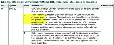
I was trying to find a solution and came across this in LPC54628 user manual:
The EMCSC bit in EMCSYSCTRL register controls whether the address output lines from the microcontroller is shifted to the right so that there is 1:1 match between the line nos of uC address lines and that of the external memory. As an example, it talks about 32bit memory chips where bit-0 of address line (A[0]) may be connected to bit-0 of external SRAM.
My query: What does this imply for 16-bit devices? If the EMCSC bit is cleared to '0' and there exists 1:1 match between A[0]:A[15] lines of microcontroller and A[0}:A[15} address line of external memory, everything should work properly, right? The PCB tracks in my board have 1:1 mapping between address lines of uC and the DPRAM.
- 新着としてマーク
- ブックマーク
- 購読
- ミュート
- RSS フィードを購読する
- ハイライト
- 印刷
- 不適切なコンテンツを報告
Hi,
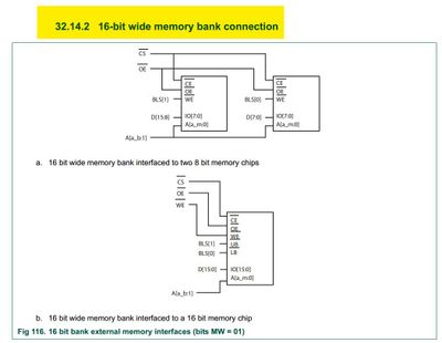
For 16 bits data width memory connection, if you connect as the Fig 116 16 bit bank external memory interfaces, obviously, the EMCSC bit must be set, because A[xxx,1] of LPC54628 are connected to A[xxx-1, 0] of 16 bits SRAM(I mean that A1 of EMC is connected to A0 of 16 bits SRAM).
If A[xxx,0] of LPC54628 are connected to A[xxx, 0] for 16 bits data width memory, the EMCSC bit must be cleared(I mean that A0 of EMC is connected to A0 of 16 bits SRAM).
Hope it can help you
BR
XiangJun Rong
- 新着としてマーク
- ブックマーク
- 購読
- ミュート
- RSS フィードを購読する
- ハイライト
- 印刷
- 不適切なコンテンツを報告
Hi,
Thanks to both of you for patiently replying to my queries.
1) In my board address lines A[xxx,0] of LPC54628 are indeed connected to A[xxx, 0] of external memory and EMCSC bit is cleared in software. So that part is okay. I just wanted to be sure about my understanding.
2) Regarding BLSN[0] & [1], if they are set to FUNC6 (EMC functionality and not GPIO) and PB bit is set, then only one out of every 256 reads succeed. But when they were made GPIO and permanently set to low, one out of every two reads became successful. I am currently probing these lines on an oscilloscope and will post my findings here in some time.
- 新着としてマーク
- ブックマーク
- 購読
- ミュート
- RSS フィードを購読する
- ハイライト
- 印刷
- 不適切なコンテンツを報告
Hi,
Can you share the SRAM schematics so that we can review the hardware connection?
BR
Xiangjun Rong
- 新着としてマーク
- ブックマーク
- 購読
- ミュート
- RSS フィードを購読する
- ハイライト
- 印刷
- 不適切なコンテンツを報告
Thanks for the revert. PFA the schematics.
Note:
1) Pins P0_5 (PO_5_EMC_I/O_3L) & P0_6 (PO_6_EMC_I/O_4L) are connected only to the DPRAM. Mentioning this so that you do not get confused as to whether they are connected elsewhere also.
2) Pin P0_4 (PO_5_EMC_I/O_2L) is connected to a push button as shown at the bottom of the image and is also used for serial programming.
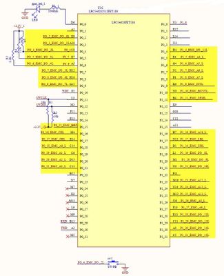
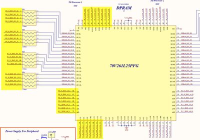
| uC signal name | Pin no | Func type | Configured as: | DPRAM signal name | Remarks |
| PO_2_EMC_I/O_0L | P0_2 | EMC_D[0] | FUNC6 | I/O_0L | |
| PO_3_EMC_I/O_1L | P0_3 | EMC_D[1] | FUNC6 | I/O_1L | |
| PO_4_EMC_I/O_2L | P0_4 | EMC_D[2] | FUNC6 | I/O_2L | |
| PO_5_EMC_I/O_3L | P0_5 | EMC_D[3] | FUNC6 | I/O_3L | |
| PO_6_EMC_I/O_4L | P0_6 | EMC_D[4] | FUNC6 | I/O_4L | |
| PO_7_EMC_I/O_5L | P0_7 | EMC_D[5] | FUNC6 | I/O_5L | |
| PO_8_EMC_I/O_6L | P0_8 | EMC_D[6] | FUNC6 | I/O_6L | |
| PO_9_EMC_I/O_7L | P0_9 | EMC_D[7] | FUNC6 | I/O_7L | |
| P1_19_EMC_I/O_8L | P1_19 | EMC_D[8] | FUNC6 | I/O_8L | |
| P1_20_EMC_I/O_9L | P1_20 | EMC_D[9] | FUNC6 | I/O_9L | |
| P1_21_EMC_I/O_10L | P1_21 | EMC_D[10] | FUNC6 | I/O_10L | |
| P1_4_EMC_I/O_11L | P1_4 | EMC_D[11] | FUNC6 | I/O_11L | |
| P1_28_EMC_I/O_12L | P1_28 | EMC_D[12] | FUNC6 | I/O_12L | |
| P1_29_EMC_I/O_13L | P1_29 | EMC_D[13] | FUNC6 | I/O_13L | |
| P1_30_EMC_I/O_14L | P1_30 | EMC_D[14] | FUNC6 | I/O_14L | |
| P1_31_EMC_I/O_15L | P1_31 | EMC_D[15] | FUNC6 | I/O_15L | |
| P0_18_EMC_A0_L | P0_18 | EMC_A[0] | FUNC6 | A0L | |
| P0_19_EMC_A1_L | P0_19 | EMC_A[1] | FUNC6 | A1L | |
| P0_20_EMC_A2_L | P0_20 | EMC_A[2] | FUNC6 | A2L | |
| P0_21_EMC_A3_L | P0_21 | EMC_A[3] | FUNC6 | A3L | |
| P1_5_EMC_A4_L | P1_5 | EMC_A[4] | FUNC6 | A4L | |
| P1_6_EMC_A5_L | P1_6 | EMC_A[5] | FUNC6 | A5L | |
| P1_7_EMC_A6_L | P1_7 | EMC_A[6] | FUNC6 | A6L | |
| P1_8_EMC_A7_L | P1_8 | EMC_A[7] | FUNC6 | A7L | |
| P1_26_EMC_A8_L | P1_26 | EMC_A[8] | FUNC6 | A8L | |
| P1_27_EMC_A9_L | P1_27 | EMC_A[9] | FUNC6 | A9L | |
| P1_16_EMC_A10_L | P1_16 | EMC_A[10] | FUNC6 | A10L | |
| P1_23_EMC_A11_L | P1_23 | EMC_A[11] | FUNC6 | A11L | |
| P1_24_EMC_A12_L | P1_24 | EMC_A[12] | FUNC6 | A12L | |
| P1_25_EMC_A13_L | P1_25 | EMC_A[13] | FUNC6 | A13L | |
| P0_15_EMC_RWL | P0_15 | EMC_WEN | FUNC6 | R_/W | |
| P0_16_EMC_CEL | P0_16 | EMC_CSN[0] | FUNC6 | /CE_L | |
| P0_16_EMC_OEL | P0_17 | EMC_OEN | FUNC6 | /OE_L | |
| P1_9_EMC_INTL | P1_9 | EMC_CASN | - | /INT_L | Not used & not configured in software |
| P1_10_EMC_BUSYL | P1_10 | EMC_RASN | GPIO/FUNC0 | /BUSY_L | Output, Always high |
| P1_11_EMC_SEML | P1_11 | EMC_CLK[0] | GPIO/FUNC0 | /SEM_L | Output, Always high |
| P1_17_EMC_LBL | P1_17 | EMC_BLSN[0] | FUNC6 | /LB_L | |
| P1_18_EMC_UBL | P1_18 | EMC_BLSN[1] | FUNC6 | /UB_L |
- 新着としてマーク
- ブックマーク
- 購読
- ミュート
- RSS フィードを購読する
- ハイライト
- 印刷
- 不適切なコンテンツを報告
This sounds like you are missing one interface line in the config (pin_mux.c), perhaps an address line.
- 新着としてマーク
- ブックマーク
- 購読
- ミュート
- RSS フィードを購読する
- ハイライト
- 印刷
- 不適切なコンテンツを報告
Pin configuration. Please note that I am manually configuring each pin instead of using pin_mux.c. All pins are multiplexed as FUNC6 type (EMC function).
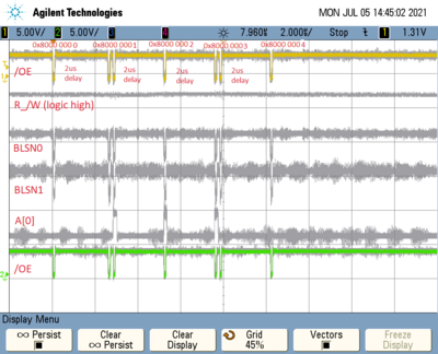
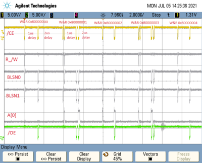
Please find attached signals as probed on oscilloscope. All pins are configured as EMC (including BLSN0 & 1).
In the 1st image, write followed by read of the same location, with a delay of 1us in between is shown. This is done for the first 5 locations in DPRAM ie, 0x8000 0000 to 0x8000 0004 in EMC. Data is '0' to 1st location, 1 to 2nd, 2 to 3rd etc.
In the 2nd image, after running the write/read loop once as mentioned above, the first 5 locations are read consecutively with a 2us delay in between.
Query 1: When addressing an odd location (0x8000 0001, 3, 5 etc) during both read and write cycles, why does/CE, BLSN0, BLSN1, /OE etc toggle twice but only once for even addresses? It looks as though the EMC is trying to access data in odd locations as two separate bytes. All memory reads except the last location fails in this code.
(As pointed out in an earlier response, success rate improves to 50% when BLSN0 & 1 are configured as GPIO and permanently set to logic low. But these images are for all pins configured as type EMC and no GPIO)
void DPRAM_full_emc_test_code(void){
	PRINTF("DPRAM_full_emc_test_code\r\n");

	while(1){
		DPRAM_Write_to_multiple_loc1_full_emc(0x80000000, 0, DPRAM_param, 5U);
	}
	delay_1ms(1000U);
	__DSB();
	__ISB();
}
void DPRAM_full_emc_test_code(void){
	PRINTF("DPRAM_full_emc_test_code\r\n");
        DPRAM_Write_to_multiple_loc1_full_emc(0x80000000, 0, DPRAM_param, 5U);

	delay_1ms(1000U);
	__DSB();
	__ISB();

	while(1){
		DPRAM_read_from_multiple_loc1_full_emc(0x80000000, 0, DPRAM_param, 5U);
		delay_1ms(1U);
	}
}
These are the contents of relevant registers of EMC peripheral:
SYSCON->EMCSYSCTRL: 0x4 // EMCSC bit = 0, burst disabled, EMC clk source is internal loop feedback of EMC_CLK output
EMC->CONTROL: 0x1 // EMC enabled, normal memory map
EMC->STATUS: 0x5 // EMC busy, write buffer empty, self-refresh mode
EMC->CONFIG: 0x0 // little endian
EMC->STATICEXTENDEDWAIT: 0x0
EMC->STATIC[0].STATICCONFIG: 0x81 // 16-bit, page mode disabled, active low chip select, PB bit = 1, extended wait disabled, buffer disabled, writes not protected
EMC->STATIC[0].STATICWAITWEN: 0x0
EMC->STATIC[0].STATICWAITOEN: 0x1
EMC->STATIC[0].STATICWAITRD: 0x4
EMC->STATIC[0].STATICWAITPAGE: 0x0
EMC->STATIC[0].STATICWAITWR: 0x0
EMC->STATIC[0].STATICWAITTURN: 0x0
DPRAM_full_emc_test_code
Ok, p=0, rb_val: 0x0, Add: 0x80000000
Ok, p=1, rb_val: 0x1, Add: 0x80000001
Ok, p=2, rb_val: 0x2, Add: 0x80000002
Ok, p=3, rb_val: 0x3, Add: 0x80000003
Ok, p=4, rb_val: 0x4, Add: 0x80000004
W&R complete


Mismatch, 0, 256, x80000000
Mismatch, 1, 513, x80000001
Mismatch, 2, 770, x80000002
Mismatch, 3, 1027, x80000003
Ok, p=4, rb_val: 0x4, Add: 0x80000004  // last location is a success! Wonder why.
- 新着としてマーク
- ブックマーク
- 購読
- ミュート
- RSS フィードを購読する
- ハイライト
- 印刷
- 不適切なコンテンツを報告
To be honest, I did not look into much details of this topic yet.
The LPCXpresso54628 board has external SDRAM using a 16-bit bus, so the schematics might help you. The lower address pins are wired directly, i.e. A0 from the MCU is wired to A0 at the DRAM.
Often, the lowest address bits are used for CS signal generation, if two/four 8-bit or two 16-bit devices are used in parallel. This seems not the case here.
The regarding code in a EMC SDK example says this:
SYSCON->EMCSYSCTRL = SYSCON_EMCSYSCTRL_EMCFBCLKINSEL(config->fbClkSrc);
were the macro evaluates to:
(((uint32_t)(((uint32_t)(config->fbClkSrc)) << (3U))) & (0x8U))
- 新着としてマーク
- ブックマーク
- 購読
- ミュート
- RSS フィードを購読する
- ハイライト
- 印刷
- 不適切なコンテンツを報告
> Were you able to resolve the issue? If yes, can you please share how it was resolved?
I had to add the pin initialisations for the SDRAM interface to pinmux.c to get it working. I had combined an application from 2 different SDK examples, and just had omitted the proper initialisations.
This might not be the case with your problem.
My point is - I got fooled by the caching mechanism, that showed a successful SDRAM write in the debugger, at least until the next debug step.
- 新着としてマーク
- ブックマーク
- 購読
- ミュート
- RSS フィードを購読する
- ハイライト
- 印刷
- 不適切なコンテンツを報告
Thanks for the reply.
In my case, few months ago, I was able to get DPRAM working with successful data transfers between two microcontrollers on either ports. However, for it to work, I had to configure the control pins of EMC peripheral (such as CE, OE, R/W etc) as GPIO and only address & data lines assigned to EMC peripheral functions (non-GPIO). Even in this method, successful read/ writes were happening only at even addresses of DPRAM. And so my application code is written such that only even addresses of DPRAM are used.
Now that the application code is complete, I wish to rectify this odd/even address issue such that all addresses are read/writeable and all pins are controlled automatically by EMC peripheral (no GPIO to control read/writes).
- 新着としてマーク
- ブックマーク
- 購読
- ミュート
- RSS フィードを購読する
- ハイライト
- 印刷
- 不適切なコンテンツを報告
Hi, Aswin,
how about using the code?
void DPRAM_full_emc_test_code(void){
	DP_read_after_write(0x80000000, 16384U);
	//  delay_1ms(100U);
	   __DSB();
           __ISB();
	DP_only_read(0x80000000, 16384U);

	while(1){
		__NOP();
	}
}
BR
XiangJun Rong
- 新着としてマーク
- ブックマーク
- 購読
- ミュート
- RSS フィードを購読する
- ハイライト
- 印刷
- 不適切なコンテンツを報告
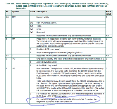
Hi,
As the following screenshot, pls refer to the PB bit, you do not need configure the EMC_BLS[1:0] as GPIO output mode, but you are required to configure the EMC_BLS[1:0] as EMC_BLS[1:0] , after you set the PB bit, the pins EMC_BLS[1:0] will function as EMC_BLS[1:0], when the core accesses the EMC, the EMC_BLS[1:0] will be low automatically.
Hope it can help you
BR
Xiangjun Rong
- 新着としてマーク
- ブックマーク
- 購読
- ミュート
- RSS フィードを購読する
- ハイライト
- 印刷
- 不適切なコンテンツを報告
You might be hunting a phantom.
I had a similar problem with the DRAM on the LPCXpresso54628 board, until I realized the pin initialisation for the DRAM interface lines were missing (in pinmux.c).
The core seems to have some caching mechanism, and I did observe seemingly successful writes to the DRAM, but the values were gone after the next debugger step.
