- Forums
- Product Forums
- General Purpose MicrocontrollersGeneral Purpose Microcontrollers
- i.MX Forumsi.MX Forums
- QorIQ Processing PlatformsQorIQ Processing Platforms
- Identification and SecurityIdentification and Security
- Power ManagementPower Management
- Wireless ConnectivityWireless Connectivity
- RFID / NFCRFID / NFC
- Advanced AnalogAdvanced Analog
- MCX Microcontrollers
- S32G
- S32K
- S32V
- MPC5xxx
- Other NXP Products
- S12 / MagniV Microcontrollers
- Powertrain and Electrification Analog Drivers
- Sensors
- Vybrid Processors
- Digital Signal Controllers
- 8-bit Microcontrollers
- ColdFire/68K Microcontrollers and Processors
- PowerQUICC Processors
- OSBDM and TBDML
- S32M
- S32Z/E
-
- Solution Forums
- Software Forums
- MCUXpresso Software and ToolsMCUXpresso Software and Tools
- CodeWarriorCodeWarrior
- MQX Software SolutionsMQX Software Solutions
- Model-Based Design Toolbox (MBDT)Model-Based Design Toolbox (MBDT)
- FreeMASTER
- eIQ Machine Learning Software
- Embedded Software and Tools Clinic
- S32 SDK
- S32 Design Studio
- GUI Guider
- Zephyr Project
- Voice Technology
- Application Software Packs
- Secure Provisioning SDK (SPSDK)
- Processor Expert Software
- Generative AI & LLMs
-
- Topics
- Mobile Robotics - Drones and RoversMobile Robotics - Drones and Rovers
- NXP Training ContentNXP Training Content
- University ProgramsUniversity Programs
- Rapid IoT
- NXP Designs
- SafeAssure-Community
- OSS Security & Maintenance
- Using Our Community
-
- Cloud Lab Forums
-
- Knowledge Bases
- ARM Microcontrollers
- i.MX Processors
- Identification and Security
- Model-Based Design Toolbox (MBDT)
- QorIQ Processing Platforms
- S32 Automotive Processing Platform
- Wireless Connectivity
- CodeWarrior
- MCUXpresso Suite of Software and Tools
- MQX Software Solutions
- RFID / NFC
- Advanced Analog
-
- NXP Tech Blogs
- Home
- :
- 汎用マイクロコントローラ
- :
- LPCマイクロコントローラ
- :
- ADCCLKSEL function in LPC804
ADCCLKSEL function in LPC804
- RSS フィードを購読する
- トピックを新着としてマーク
- トピックを既読としてマーク
- このトピックを現在のユーザーにフロートします
- ブックマーク
- 購読
- ミュート
- 印刷用ページ
ADCCLKSEL function in LPC804
- 新着としてマーク
- ブックマーク
- 購読
- ミュート
- RSS フィードを購読する
- ハイライト
- 印刷
- 不適切なコンテンツを報告
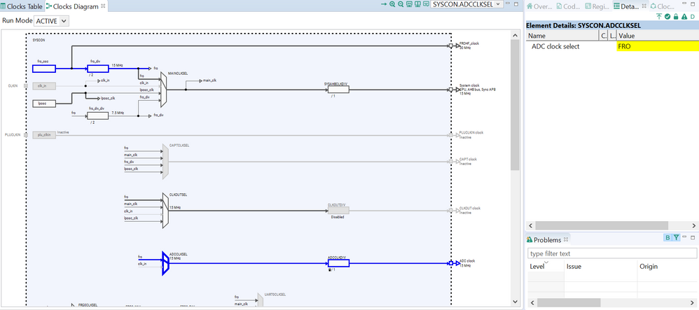
The LPC804 appears to contain the following two ADC clocks:
1.Figure 6 on page 52 of UM11065 rev 1.3 shows ADCCLKSRC, ADCCLKDIV originating from the FRO or external clock.
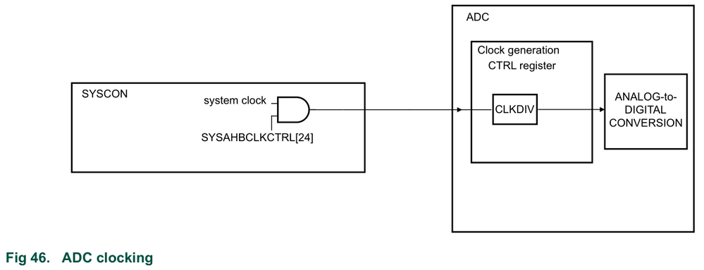
2. Figure 45 on page 279 shows the SYSAHBCLKCTRL[24] register interface clock originating from the AHB system clock.
In my testing the AHB system clock appears to be clock the conversion and without the register interface clock gated the ADC does operate (external triggers do not work). Disabling ADCCLKSRC or ADCCLKDIV has no apparent effect and the recommended initialization sequence (22.3.1 at page 279) does not initialize ADCCLKDIV from the off reset value.
What is the function of the second clock (ADCCLKSRC) in the LPC804?
- 新着としてマーク
- ブックマーク
- 購読
- ミュート
- RSS フィードを購読する
- ハイライト
- 印刷
- 不適切なコンテンツを報告
Hello Johan Forslöf
The LPC804 ADC has two clock sources, the FRO clock, and an external clock. If you are using the device SDK you can select the clock source with the function CLOCK_Select(). As a parameter, you can put "kADC_Clk_From_Fro" or "kADC_Clk_From_Extclk".
The reason to use an external clock may vary depending on your application, one reason might be precision since the internal clocks can vary its precision with temperature changes.
Let me know if this is helpful, if you have more questions do not hesitate to ask me.
Best regards,
Omar
- 新着としてマーク
- ブックマーク
- 購読
- ミュート
- RSS フィードを購読する
- ハイライト
- 印刷
- 不適切なコンテンツを報告
Hello Omar and thank you for your swift response!
I can see why an external clock may be useful but I fear that I am still confused. The clocking diagram on page 279 of UM11065 rev.3 shows a completely different clock tree derived from the system clock instead of the FRO or external clock input:
Why are there two different clock trees and what are they used for? In my tests the ADC operates normally even with ADCLKSEL set to "none".
The reason I ask is that I originally thought clock generated by the ADCCLKSEL multiplexer was the only one used and spent longer than I'd like to admit debugging a race condition where the register interface clock (bit 24 of SYSAHBCLKCTRL above) was sometimes temporarily masked in an interrupt, during which time external triggers do not work.
To avoid future trouble I would therefore like to clear up what the these two clocks are used for.
Regards,
Johan
- 新着としてマーク
- ブックマーク
- 購読
- ミュート
- RSS フィードを購読する
- ハイライト
- 印刷
- 不適切なコンテンツを報告
Hello Johan Forslöf
I apology the inconvenience this is causing you. Allow me to clarify this.
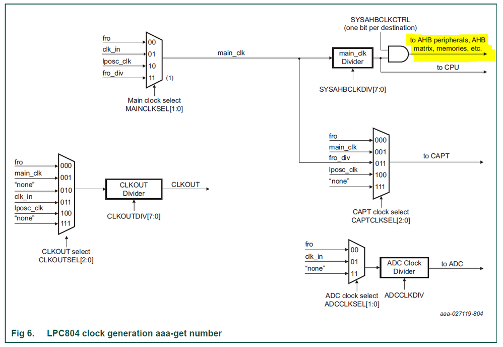
We can use this image for reference:
The signal that goes to the APB bridge that I highlighted in yellow is the signal that clock gates the ADC with the SYSAHBCLKCTRL register however to a proper function of the ADC we need a clock source to control the conversions.
These two sources can be the FRO or an external oscillator and are selected with ADCCLKSEL register, if no clock is selected then the ADC will not work as expected.
Let me know if this is helpful, if you have more questions do not hesitate to ask me.
Best regards,
Omar


