
- NXP Forums
- Product Forums
- General Purpose MicrocontrollersGeneral Purpose Microcontrollers
- i.MX Forumsi.MX Forums
- QorIQ Processing PlatformsQorIQ Processing Platforms
- Identification and SecurityIdentification and Security
- Power ManagementPower Management
- MCX Microcontrollers
- S32G
- S32K
- S32V
- MPC5xxx
- Other NXP Products
- Wireless Connectivity
- S12 / MagniV Microcontrollers
- Powertrain and Electrification Analog Drivers
- Sensors
- Vybrid Processors
- Digital Signal Controllers
- 8-bit Microcontrollers
- ColdFire/68K Microcontrollers and Processors
- PowerQUICC Processors
- OSBDM and TBDML
-
- Solution Forums
- Software Forums
- MCUXpresso Software and ToolsMCUXpresso Software and Tools
- CodeWarriorCodeWarrior
- MQX Software SolutionsMQX Software Solutions
- Model-Based Design Toolbox (MBDT)Model-Based Design Toolbox (MBDT)
- FreeMASTER
- eIQ Machine Learning Software
- Embedded Software and Tools Clinic
- S32 SDK
- S32 Design Studio
- Vigiles
- GUI Guider
- Zephyr Project
- Voice Technology
- Application Software Packs
- Secure Provisioning SDK (SPSDK)
- Processor Expert Software
-
- Topics
- Mobile Robotics - Drones and RoversMobile Robotics - Drones and Rovers
- NXP Training ContentNXP Training Content
- University ProgramsUniversity Programs
- Rapid IoT
- NXP Designs
- SafeAssure-Community
- OSS Security & Maintenance
- Using Our Community
-
- Cloud Lab Forums
-
- Home
- :
- 汎用マイクロコントローラ
- :
- Kinetisマイクロコントローラ
- :
- default pin status after reset
default pin status after reset
- RSS フィードを購読する
- トピックを新着としてマーク
- トピックを既読としてマーク
- このトピックを現在のユーザーにフロートします
- ブックマーク
- 購読
- ミュート
- 印刷用ページ
- 新着としてマーク
- ブックマーク
- 購読
- ミュート
- RSS フィードを購読する
- ハイライト
- 印刷
- 不適切なコンテンツを報告
Dear Support,
I am a little confused about the status during the chip is holding in reset mode.
in K24P144M120SF5, Rev 5, 12/2014
chapter 5.1 there is a column called Default, is this the pin definition when chip is hold in reset mode.
what is the difference between Default and ALT0. noticed that all DISABLED pins in Default column, there are empty in ALT0 column.
is the DISABLED means the pin is put in Hi-Impedance( disconnected).
in K24 Sub-Family Reference Manual(K24p144M120SF5RM.
in table 10-2, Pin mux at reset. most of the port are ALT0.
Here is why I ask this question. in our design, we connected Pin C4 and D5 to a uart port. I want to know what is the status ( voltage level if we have 1M ohm pull down resistor) during reset.
second question is if the chip is brand new, not programmed. what is the pin C4 and D5 status after reset?
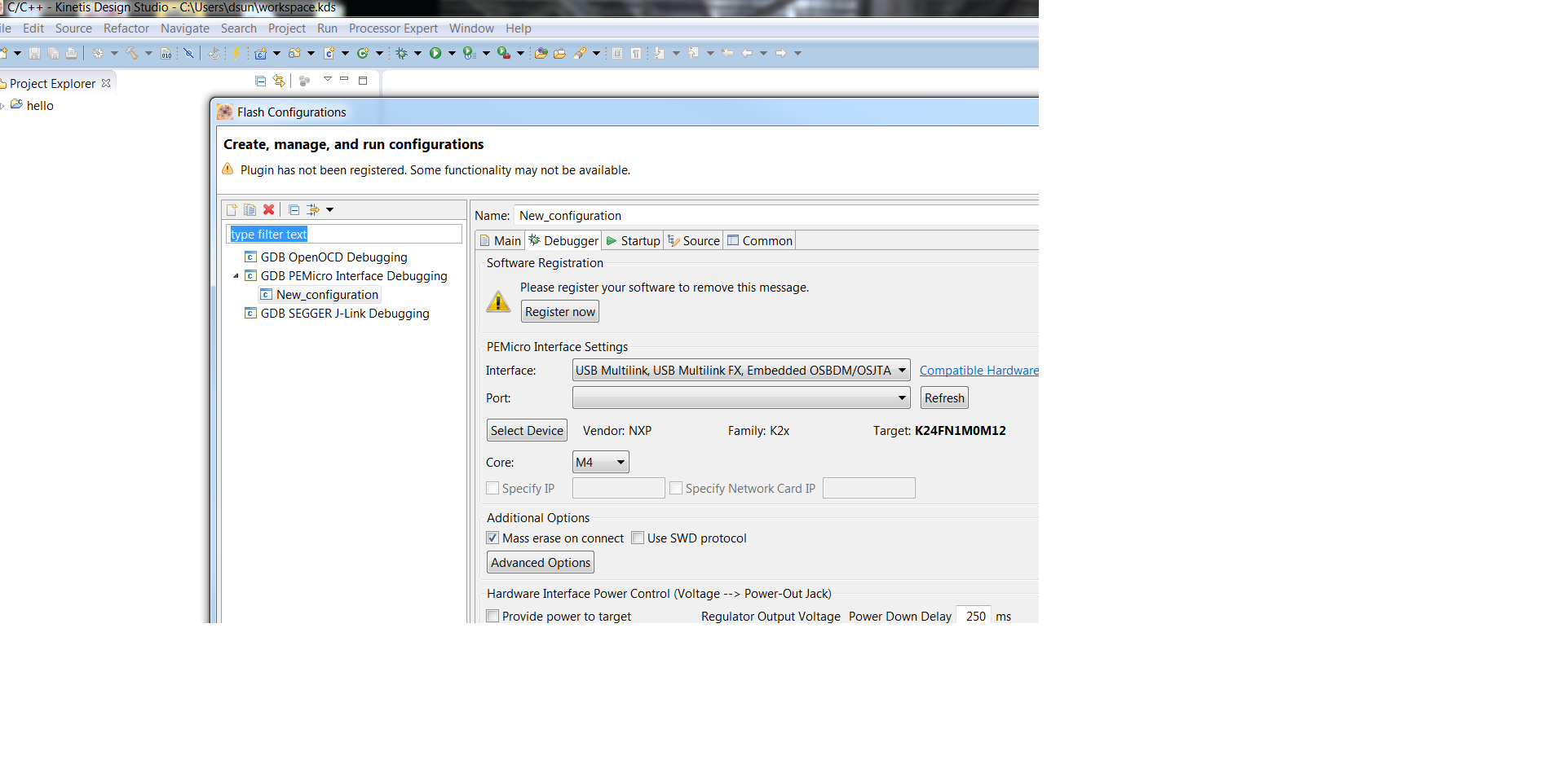
third question, if I use freescale KDS 3.2.0. "flash from file function", in Debugger function. I checked "Mass erase on connect" without any "preserve" and didn't assign a symbols or a file in Startup Menu. if I execute Flash. I believe the tools will do a "mass erase on connect" and failed to flash a new image to the chip.
is the chip in default factory status after this mass erase? what is the expectation of the pins out of reset? if the chip is in a unknown status, is there a simple way to reset the chip to factory default use Freescale KDS or any other tools?
thanks,
David Sun
解決済! 解決策の投稿を見る。
- 新着としてマーク
- ブックマーク
- 購読
- ミュート
- RSS フィードを購読する
- ハイライト
- 印刷
- 不適切なコンテンツを報告
Hi, David
Regarding the pin status during and after Reset, pls refer to section 10.3.1 K24 Signal Multiplexing and Pin Assignments in RM of K24. In detail, all analog pins remain the ananlog function. For digital pins, the JTAG pins remain the JTAG function, for the other digital pins, they are disabled, in other words in high impedance. If you have doubts, pls list the pins you have doubts.
After mass erase, all the flash are empty(0xFF) and all flash are in unsecurity state, which is equivalent to a factory default chip.
Hope it can help you
BR
Xiangjun Rong
- 新着としてマーク
- ブックマーク
- 購読
- ミュート
- RSS フィードを購読する
- ハイライト
- 印刷
- 不適切なコンテンツを報告
Hi XiangJun Rong,
The last question is not clear to me. if I did a mass erase to the chip. is it equivalent to a factory default chip? what is the pin status during and after the reset?
thanks,
David Sun
- 新着としてマーク
- ブックマーク
- 購読
- ミュート
- RSS フィードを購読する
- ハイライト
- 印刷
- 不適切なコンテンツを報告
Hi, David
Regarding the pin status during and after Reset, pls refer to section 10.3.1 K24 Signal Multiplexing and Pin Assignments in RM of K24. In detail, all analog pins remain the ananlog function. For digital pins, the JTAG pins remain the JTAG function, for the other digital pins, they are disabled, in other words in high impedance. If you have doubts, pls list the pins you have doubts.
After mass erase, all the flash are empty(0xFF) and all flash are in unsecurity state, which is equivalent to a factory default chip.
Hope it can help you
BR
Xiangjun Rong
- 新着としてマーク
- ブックマーク
- 購読
- ミュート
- RSS フィードを購読する
- ハイライト
- 印刷
- 不適切なコンテンツを報告
thank you very much.
- 新着としてマーク
- ブックマーク
- 購読
- ミュート
- RSS フィードを購読する
- ハイライト
- 印刷
- 不適切なコンテンツを報告
Hi, David,
I think the default state is the state that the chip is during Reset and after Reset until code is executed to configure the pin to a function. The "disabled" is in high impedance.
Regarding the image you attached, if you check the "mass erase" box, the tools will mass erase the flash when you download code. Once you erase the flash, you can not recover it.
Hope it can help you
BR
XiangJun Rong