- Forums
- Product Forums
- General Purpose MicrocontrollersGeneral Purpose Microcontrollers
- i.MX Forumsi.MX Forums
- QorIQ Processing PlatformsQorIQ Processing Platforms
- Identification and SecurityIdentification and Security
- Power ManagementPower Management
- Wireless ConnectivityWireless Connectivity
- RFID / NFCRFID / NFC
- Advanced AnalogAdvanced Analog
- MCX Microcontrollers
- S32G
- S32K
- S32V
- MPC5xxx
- Other NXP Products
- S12 / MagniV Microcontrollers
- Powertrain and Electrification Analog Drivers
- Sensors
- Vybrid Processors
- Digital Signal Controllers
- 8-bit Microcontrollers
- ColdFire/68K Microcontrollers and Processors
- PowerQUICC Processors
- OSBDM and TBDML
- S32M
- S32Z/E
-
- Solution Forums
- Software Forums
- MCUXpresso Software and ToolsMCUXpresso Software and Tools
- CodeWarriorCodeWarrior
- MQX Software SolutionsMQX Software Solutions
- Model-Based Design Toolbox (MBDT)Model-Based Design Toolbox (MBDT)
- FreeMASTER
- eIQ Machine Learning Software
- Embedded Software and Tools Clinic
- S32 SDK
- S32 Design Studio
- GUI Guider
- Zephyr Project
- Voice Technology
- Application Software Packs
- Secure Provisioning SDK (SPSDK)
- Processor Expert Software
- Generative AI & LLMs
-
- Topics
- Mobile Robotics - Drones and RoversMobile Robotics - Drones and Rovers
- NXP Training ContentNXP Training Content
- University ProgramsUniversity Programs
- Rapid IoT
- NXP Designs
- SafeAssure-Community
- OSS Security & Maintenance
- Using Our Community
-
- Cloud Lab Forums
-
- Knowledge Bases
- ARM Microcontrollers
- i.MX Processors
- Identification and Security
- Model-Based Design Toolbox (MBDT)
- QorIQ Processing Platforms
- S32 Automotive Processing Platform
- Wireless Connectivity
- CodeWarrior
- MCUXpresso Suite of Software and Tools
- MQX Software Solutions
- RFID / NFC
- Advanced Analog
-
- NXP Tech Blogs
- Home
- :
- General Purpose Microcontrollers
- :
- Kinetis Microcontrollers
- :
- TWR-K40D100M / TWR-SER FlexCAN issues
TWR-K40D100M / TWR-SER FlexCAN issues
- Subscribe to RSS Feed
- Mark Topic as New
- Mark Topic as Read
- Float this Topic for Current User
- Bookmark
- Subscribe
- Mute
- Printer Friendly Page
TWR-K40D100M / TWR-SER FlexCAN issues
- Mark as New
- Bookmark
- Subscribe
- Mute
- Subscribe to RSS Feed
- Permalink
- Report Inappropriate Content
Hello,
I've been having some trouble with sending out a CAN message from the TWR-SER board using the TWR-K40100M module on an actual CAN network (not in loopback mode).
Details:
Kinetis Design Studio 3.2.0
Processor Expert
CAN_LDD bean
TWR-K40D100M
TWR-SER
I am trying to achieve a successful CAN message transmission from the TWR-SER to an external CAN node.
The test network is terminated at both ends (at the TWR-SER board and at the CANbus monitor device)!
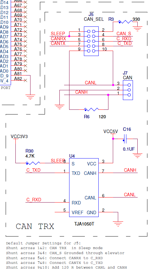
On the TWR-SER module
- J5 is configured as follows:
- 1->2 shorted (CAN transceiver full power mode)
- Refer to Robert's reply in https://community.nxp.com/message/104118?commentID=104118#comment-104118
- 3->4 shorted (CAN_S grounded to TWR-SER board
- 5->6 shorted (C_RXD to CANRX)
- 7->8 shorted (C_TXD to CANTX)
- 9->10 shorted (120ohm term on TWR-SER)
- 1->2 shorted (CAN transceiver full power mode)
-------------------------------------------------------------------------------------------------------------------------
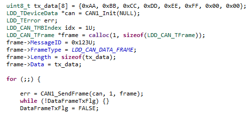
in main.c
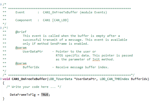
in Events.c:
On the K40D100M
- Followed the example FlexCAN initialization from the help document
- Interrupt-driven TX transfer (using Events.c)
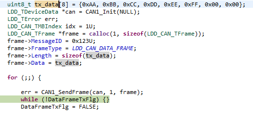
When I initiate a CAN transmit message, the function returns an error code of 0 (ERR_OK), but then the program would hang at the while loop checking DataFrameTxFlg. During debugging, CAN1_OnFreeTx_Buffer never triggers. The entire hardware configuration is correct (as far as I know). The FlexCAN software initialization seems to be correct, but the CAN1_OnFreeTx_Buffer not triggering I am still unsure about.
Attached is my project.
Any advice / guidance is appreciated!
Efren
Original Attachment has been moved to: BMS_Controller.zip
- Mark as New
- Bookmark
- Subscribe
- Mute
- Subscribe to RSS Feed
- Permalink
- Report Inappropriate Content
Update: I placed a scope probe on the CANTX header pin on the TWR-SER board (which connects to PTE_24 (configured as CAN_TX) on the TWR-K40D100 board.
- The scope shows no signal activity when calling CAN1_SendTxFrame. I've verified from PTE_24 (CAN1_TX) / PTE_25 (CAN1_RX) on the TWR-K40D100M board to J5 pin 7 (CAN_TX) / J5 pin 5 (CAN_RX) the TWR-SER board.
- I have good confidence that the TJA1050T CAN module does work, as I sent an artificial msg over CAN and see activity on J5 pin 6 (C_RXD).
So it leads to a few possible scenarios:
- The CAN1 peripheral is not configured correctly (even using Processor Expert.
- Somewhere from the expansion contacts to the MCU itself there is a discontinuity.
Here is the CAN1 CAN_LDD header showing CAN1 configuration:
/* ###################################################################
** This component module is generated by Processor Expert. Do not modify it.
** Filename : CAN1.c
** Project : BMS_Controller
** Processor : MK40DX256VMD10
** Component : CAN_LDD
** Version : Component 01.112, Driver 01.07, CPU db: 3.00.000
** Repository : Kinetis
** Compiler : GNU C Compiler
** Date/Time : 2016-09-28, 13:04, # CodeGen: 67
** Abstract :
** This component "CAN_LDD" implements a CAN serial channel.
** Settings :
** Component name : CAN1
** CAN channel : CAN1
** Interrupt service : Enabled
** Interrupt error : INT_CAN1_Error
** Interrupt error priority : medium priority
** Interrupt bus off : INT_CAN1_Bus_Off
** Interrupt bus off priority : medium priority
** Interrupt message buffers : INT_CAN1_ORed_Message_buffer
** Interrupt message buffers priority : medium priority
** Interrupt Tx warning : INT_CAN1_Tx_Warning
** Interrupt Tx warning priority : medium priority
** Interrupt Rx warning : INT_CAN1_Rx_Warning
** Interrupt Rx warning priority : medium priority
** Interrupt wake up : INT_CAN1_Wake_Up
** Interrupt wake up priority : medium priority
** Settings :
** Pins :
** Rx pin :
** Rx pin : ADC0_SE18/PTE25/CAN1_RX/UART4_RX/FB_AD23/EWM_IN
** Rx pin signal : CAN1_RX
** Tx pin :
** Tx pin : ADC0_SE17/PTE24/CAN1_TX/UART4_TX/EWM_OUT_b
** Tx pin Signal : CAN1_TX
** Global acceptance mask : yes
** Acceptance mask for buffer 0 .. n : 0x1FFFFFFF
** Acceptance mask for buffer 14 : 0x1FFFFFFF
** Acceptance mask for buffer 15 : 0x1FFFFFFF
** Receiver FIFO : Disabled
** Message buffers : 2
** Buffer0 :
** Buffer type : Receive
** Accept frames : Standard
** Message ID : 0x7FF
** Invidual Acceptance Mask : Disabled
** Buffer1 :
** Buffer type : Transmit
** Abort transmission mode : no
** Remote request storing : Remote Request Frame is stored
** Entire frame arbitration field comparison : no
** Local priority : no
** Self reception : Disabled
** Timer synchronization : Disabled
** Lowest buffer transmitted first : Lowest ID
** Loop mode : no
** Bus off recovery mode : Automatic
** Listen only mode : no
** Wake up : Disabled
** Timing :
** CAN timing calculator : click to run ->
** Propagation segment : 5
** Time segment 1 : 8
** Time segment 2 : 2
** Resync jump width : 1
** Time quanta per bit : 16
** Samples per bit : One sample
** Bit rate : 250 kbit/s
** Initialization :
** Enabled in init. code : yes
** Auto initialization : no
** Event mask :
** OnFreeTxBuffer : Enabled
** OnFullRxBuffer : Enabled
** OnTransmitWarning : Disabled
** OnReceiveWarning : Disabled
** OnBusOff : Disabled
** OnWakeUp : Disabled
** OnError : Disabled
** CPU clock/configuration selection :
** Clock configuration 0 : This component enabled
** Clock configuration 1 : This component disabled
** Clock configuration 2 : This component disabled
** Clock configuration 3 : This component disabled
** Clock configuration 4 : This component disabled
** Clock configuration 5 : This component disabled
** Clock configuration 6 : This component disabled
** Clock configuration 7 : This component disabled
** Contents :
** Init - LDD_TDeviceData* CAN1_Init(LDD_TUserData *UserDataPtr);
** Deinit - void CAN1_Deinit(LDD_TDeviceData *DeviceDataPtr);
** Enable - LDD_TError CAN1_Enable(LDD_TDeviceData *DeviceDataPtr);
** Disable - LDD_TError CAN1_Disable(LDD_TDeviceData *DeviceDataPtr);
** SetRxBufferID - LDD_TError CAN1_SetRxBufferID(LDD_TDeviceData *DeviceDataPtr,...
** SendFrame - LDD_TError CAN1_SendFrame(LDD_TDeviceData *DeviceDataPtr, LDD_CAN_TMBIndex...
** ReadFrame - LDD_TError CAN1_ReadFrame(LDD_TDeviceData *DeviceDataPtr, LDD_CAN_TMBIndex...
**
** Copyright : 1997 - 2015 Freescale Semiconductor, Inc.
** All Rights Reserved.
**
** Redistribution and use in source and binary forms, with or without modification,
** are permitted provided that the following conditions are met:
**
** o Redistributions of source code must retain the above copyright notice, this list
** of conditions and the following disclaimer.
**
** o Redistributions in binary form must reproduce the above copyright notice, this
** list of conditions and the following disclaimer in the documentation and/or
** other materials provided with the distribution.
**
** o Neither the name of Freescale Semiconductor, Inc. nor the names of its
** contributors may be used to endorse or promote products derived from this
** software without specific prior written permission.
**
** THIS SOFTWARE IS PROVIDED BY THE COPYRIGHT HOLDERS AND CONTRIBUTORS "AS IS" AND
** ANY EXPRESS OR IMPLIED WARRANTIES, INCLUDING, BUT NOT LIMITED TO, THE IMPLIED
** WARRANTIES OF MERCHANTABILITY AND FITNESS FOR A PARTICULAR PURPOSE ARE
** DISCLAIMED. IN NO EVENT SHALL THE COPYRIGHT HOLDER OR CONTRIBUTORS BE LIABLE FOR
** ANY DIRECT, INDIRECT, INCIDENTAL, SPECIAL, EXEMPLARY, OR CONSEQUENTIAL DAMAGES
** (INCLUDING, BUT NOT LIMITED TO, PROCUREMENT OF SUBSTITUTE GOODS OR SERVICES;
** LOSS OF USE, DATA, OR PROFITS; OR BUSINESS INTERRUPTION) HOWEVER CAUSED AND ON
** ANY THEORY OF LIABILITY, WHETHER IN CONTRACT, STRICT LIABILITY, OR TORT
** (INCLUDING NEGLIGENCE OR OTHERWISE) ARISING IN ANY WAY OUT OF THE USE OF THIS
** SOFTWARE, EVEN IF ADVISED OF THE POSSIBILITY OF SUCH DAMAGE.
**
** http: www.freescale.com
** mail: support@freescale.com
** ###################################################################*/
/*!
** @file CAN1.c
** @version 01.07
** @brief
** This component "CAN_LDD" implements a CAN serial channel.
*/
/*!
** @addtogroup CAN1_module CAN1 module documentation
** @{
*/
Here is the CAN1_Init function:
LDD_TDeviceData* CAN1_Init(LDD_TUserData *UserDataPtr)
{
/* Allocate LDD device structure */
CAN1_TDeviceDataPtr DeviceDataPrv;
/* {Default RTOS Adapter} Driver memory allocation: Dynamic allocation is simulated by a pointer to the static object */
DeviceDataPrv = &DeviceDataPrv__DEFAULT_RTOS_ALLOC;DeviceDataPrv->BaseAddr = CAN1_BASE_PTR; /* Device base address*/
DeviceDataPrv->UserData = UserDataPtr; /* Store the RTOS device structure */
DeviceDataPrv->MaxDataLen = 0x08U; /* Max number of data to be sent in one frame */
DeviceDataPrv->MaxBufferIndex = (LDD_CAN_TMBIndex)(CAN1_CAN_MBUFFERS-1U); /* Number of max. message buffer index */
DeviceDataPrv->BuffersNumber = (LDD_CAN_TMBIndex)CAN1_CAN_MBUFFERS; /* Number of message buffers */
DeviceDataPrv->RxBufferMask = 0x01U; /* Bit mask for message buffers configured as receive */
DeviceDataPrv->TxBufferMask = 0x02U; /* Bit mask for message buffers configured as transmit */
DeviceDataPrv->EnUser = TRUE; /* Enable device */
/*Clock Gating initialization*/
/* SIM_SCGC3: FLEXCAN1=1 */
SIM_SCGC3 |= SIM_SCGC3_FLEXCAN1_MASK;
/* Allocate interrupt vectors */
/* {Default RTOS Adapter} Set interrupt vector: IVT is static, ISR parameter is passed by the global variable */
INT_CAN1_Error__DEFAULT_RTOS_ISRPARAM = DeviceDataPrv;
/* {Default RTOS Adapter} Set interrupt vector: IVT is static, ISR parameter is passed by the global variable */
INT_CAN1_Bus_Off__DEFAULT_RTOS_ISRPARAM = DeviceDataPrv;
/* {Default RTOS Adapter} Set interrupt vector: IVT is static, ISR parameter is passed by the global variable */
INT_CAN1_ORed_Message_buffer__DEFAULT_RTOS_ISRPARAM = DeviceDataPrv;
/* {Default RTOS Adapter} Set interrupt vector: IVT is static, ISR parameter is passed by the global variable */
INT_CAN1_Tx_Warning__DEFAULT_RTOS_ISRPARAM = DeviceDataPrv;
/* {Default RTOS Adapter} Set interrupt vector: IVT is static, ISR parameter is passed by the global variable */
INT_CAN1_Rx_Warning__DEFAULT_RTOS_ISRPARAM = DeviceDataPrv;
/* {Default RTOS Adapter} Set interrupt vector: IVT is static, ISR parameter is passed by the global variable */
INT_CAN1_Wake_Up__DEFAULT_RTOS_ISRPARAM = DeviceDataPrv;/* initialization of CAN RX pin¨*/
/* PORTE_PCR25: ISF=0,MUX=2 */
PORTE_PCR25 = (uint32_t)((PORTE_PCR25 & (uint32_t)~(uint32_t)(
PORT_PCR_ISF_MASK |
PORT_PCR_MUX(0x05)
)) | (uint32_t)(
PORT_PCR_MUX(0x02)
));
PORT_PDD_SetPinPullSelect(PORTE_BASE_PTR, 25, PORT_PDD_PULL_UP);
PORT_PDD_SetPinPullEnable(PORTE_BASE_PTR, 25, PORT_PDD_PULL_ENABLE);
/* initialization of CAN TX pin */
/* PORTE_PCR24: ISF=0,MUX=2 */
PORTE_PCR24 = (uint32_t)((PORTE_PCR24 & (uint32_t)~(uint32_t)(
PORT_PCR_ISF_MASK |
PORT_PCR_MUX(0x05)
)) | (uint32_t)(
PORT_PCR_MUX(0x02)
));
PORT_PDD_SetPinPullSelect(PORTE_BASE_PTR, 24, PORT_PDD_PULL_UP);
PORT_PDD_SetPinPullEnable(PORTE_BASE_PTR, 24, PORT_PDD_PULL_ENABLE);
/*Interrupt priorities*/
/* NVICIP39: PRI39=0x80 */
NVICIP39 = NVIC_IP_PRI39(0x80);
/* NVICISER1: SETENA|=0x80 */
NVICISER1 |= NVIC_ISER_SETENA(0x80);
/* NVICIP38: PRI38=0x80 */
NVICIP38 = NVIC_IP_PRI38(0x80);
/* NVICISER1: SETENA|=0x40 */
NVICISER1 |= NVIC_ISER_SETENA(0x40);
/* NVICIP37: PRI37=0x80 */
NVICIP37 = NVIC_IP_PRI37(0x80);
/* NVICISER1: SETENA|=0x20 */
NVICISER1 |= NVIC_ISER_SETENA(0x20);
/* NVICIP40: PRI40=0x80 */
NVICIP40 = NVIC_IP_PRI40(0x80);
/* NVICISER1: SETENA|=0x0100 */
NVICISER1 |= NVIC_ISER_SETENA(0x0100);
/* NVICIP41: PRI41=0x80 */
NVICIP41 = NVIC_IP_PRI41(0x80);
/* NVICISER1: SETENA|=0x0200 */
NVICISER1 |= NVIC_ISER_SETENA(0x0200);
/* NVICIP42: PRI42=0x80 */
NVICIP42 = NVIC_IP_PRI42(0x80);
/* NVICISER1: SETENA|=0x0400 */
NVICISER1 |= NVIC_ISER_SETENA(0x0400);
/* CAN1_MCR: MDIS=1 */
CAN1_MCR |= CAN_MCR_MDIS_MASK; /* Disable CAN module */
/*XTAL Clock*/
/* CAN1_CTRL1: PRESDIV=0,RJW=0,PSEG1=0,PSEG2=0,BOFFMSK=0,ERRMSK=0,CLKSRC=0,LPB=0,TWRNMSK=0,RWRNMSK=0,??=0,??=0,SMP=0,BOFFREC=0,TSYN=0,LBUF=0,LOM=0,PROPSEG=0 */
CAN1_CTRL1 = CAN_CTRL1_PRESDIV(0x00) |
CAN_CTRL1_RJW(0x00) |
CAN_CTRL1_PSEG1(0x00) |
CAN_CTRL1_PSEG2(0x00) |
CAN_CTRL1_PROPSEG(0x00);
/* CAN1_MCR: MDIS=0,SOFTRST=1 */
CAN1_MCR = (uint32_t)((CAN1_MCR & (uint32_t)~(uint32_t)(
CAN_MCR_MDIS_MASK
)) | (uint32_t)(
CAN_MCR_SOFTRST_MASK
)); /* Soft Reset */
while (CAN_PDD_GetSoftResetState(CAN1_BASE_PTR) == CAN_PDD_NOT_RESET){} /* Wait for Soft reset Acknowledge */
while (CAN_PDD_GetFreezeAck(CAN1_BASE_PTR) == CAN_PDD_NOT_FREEZE){} /* Wait for entering the freeze mode */
/* CAN1_MCR: WRNEN=1,SRXDIS=1,MAXMB&=~0x0E,MAXMB|=1 */
CAN1_MCR = (uint32_t)((CAN1_MCR & (uint32_t)~(uint32_t)(
CAN_MCR_MAXMB(0x0E)
)) | (uint32_t)(
CAN_MCR_WRNEN_MASK |
CAN_MCR_SRXDIS_MASK |
CAN_MCR_MAXMB(0x01)
)); /* MCR reg. Settings */
/* CAN1_CTRL1: PRESDIV|=1,PSEG1=7,PSEG2|=1,LBUF=1,PROPSEG|=4 */
CAN1_CTRL1 |= CAN_CTRL1_PRESDIV(0x01) |
CAN_CTRL1_PSEG1(0x07) |
CAN_CTRL1_PSEG2(0x01) |
CAN_CTRL1_LBUF_MASK |
CAN_CTRL1_PROPSEG(0x04); /* Setting CTRL1 register */
/* CAN1_CTRL2: RRS=1 */
CAN1_CTRL2 |= CAN_CTRL2_RRS_MASK; /* Setting CTRL2 register */
/* CAN1_RXMGMASK: MG=0x1FFFFFFF */
CAN1_RXMGMASK = CAN_RXMGMASK_MG(0x1FFFFFFF); /* Set the Global acceptance mask register */
/* CAN1_RX14MASK: RX14M=0x1FFFFFFF */
CAN1_RX14MASK = CAN_RX14MASK_RX14M(0x1FFFFFFF); /* Set the acceptance mask register for buffers 14 */
/* CAN1_RX15MASK: RX15M=0x1FFFFFFF */
CAN1_RX15MASK = CAN_RX15MASK_RX15M(0x1FFFFFFF); /* Set the acceptance mask register for buffers 15 */
/* Initialize the message buffer 0 - Rx */
CAN_PDD_SetMessageBufferCode(CAN1_BASE_PTR, 0U, CAN_PDD_MB_RX_NOT_ACTIVE);
CAN_PDD_EnableMessageBufferIDExt(CAN1_BASE_PTR, 0U, PDD_DISABLE); /* Extended Frame bit IDE clear*/
CAN_PDD_SetMessageBufferID(CAN1_BASE_PTR, 0U, CAN_PDD_BUFFER_ID_STD, 0x07FFU); /* Set standard buffer ID */
CAN_PDD_SetMessageBufferCode(CAN1_BASE_PTR, 0U, CAN_PDD_MB_RX_EMPTY); /* Empty Frame*/
CAN_PDD_EnableMessageBufferSRR(CAN1_BASE_PTR, 0U, PDD_DISABLE); /* SRR set to 0 */
CAN_PDD_EnableMessageBufferRTR(CAN1_BASE_PTR, 0U, PDD_DISABLE); /* RTR set to 0*/
CAN_PDD_SetMessageBufferWORD0(CAN1_BASE_PTR, 0U, 0x00U); /*Clear Data field*/
CAN_PDD_SetMessageBufferWORD1(CAN1_BASE_PTR, 0U, 0x00U); /*Clear Data field*/
CAN_PDD_SetMessageBufferTimeStamp(CAN1_BASE_PTR, 0U, 0x00U); /* Empty Frame*/
/* Initialize the message buffer 1 - Tx */
CAN_PDD_SetMessageBufferCode(CAN1_BASE_PTR, 1U, CAN_PDD_MB_TX_NOT_ACTIVE); /* Control/status word to hold Tx message buffer 1 inactive */
CAN_PDD_EnableMessageBufferSRR(CAN1_BASE_PTR, 1U, PDD_DISABLE); /* SRR set to 0 */
CAN_PDD_EnableMessageBufferRTR(CAN1_BASE_PTR, 1U, PDD_DISABLE); /* RTR set to 0*/
CAN_PDD_SetMessageBufferWORD0(CAN1_BASE_PTR, 1U, 0x00U); /*Clear Data field*/
CAN_PDD_SetMessageBufferWORD1(CAN1_BASE_PTR, 1U, 0x00U); /*Clear Data field*/
CAN_PDD_SetMessageBufferTimeStamp(CAN1_BASE_PTR, 1U, 0x00U); /* Empty Frame*/
HWEnDi(DeviceDataPrv); /* Enable/disable device according to status flags */
/* Registration of the device structure */
PE_LDD_RegisterDeviceStructure(PE_LDD_COMPONENT_CAN1_ID,DeviceDataPrv);
return ((LDD_TDeviceDataPtr)DeviceDataPrv);
}
- Mark as New
- Bookmark
- Subscribe
- Mute
- Subscribe to RSS Feed
- Permalink
- Report Inappropriate Content
Hi,
As an alternative, can you use the SDK2.0 based on K40 processor? there is FlexCAN example in SDK2.0
you can download SDK2.0 from the website:
BR
Xiangjun Rong
- Mark as New
- Bookmark
- Subscribe
- Mute
- Subscribe to RSS Feed
- Permalink
- Report Inappropriate Content
Hi,
I think the jumper is okay to close all J5 on the TWR-SER board.
I have downloaded your code, but I faced some error when I compile and download. Anyway, can you check the CAN1 register to check whether the CAN1 register has be written?
BR
XiangJun Rong
- Mark as New
- Bookmark
- Subscribe
- Mute
- Subscribe to RSS Feed
- Permalink
- Report Inappropriate Content
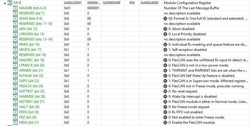
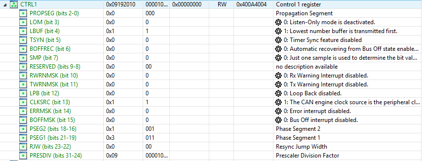
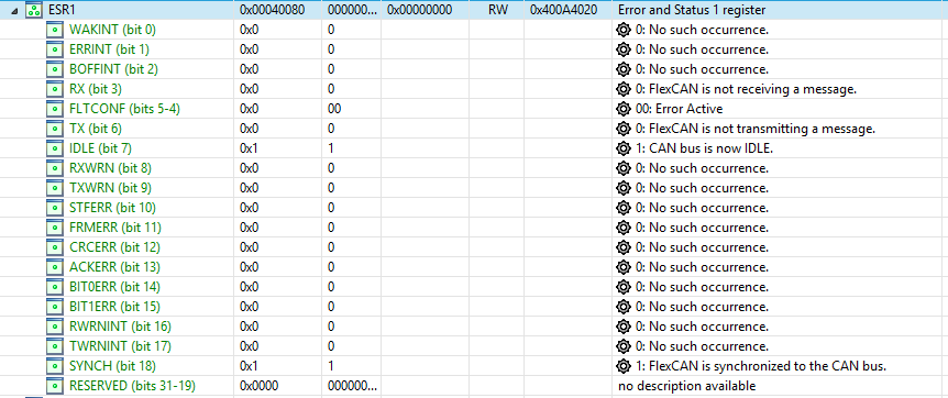
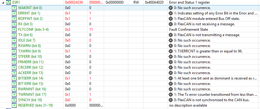
Hi Xiangjun,
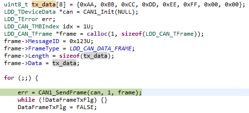
Here are pictures of the relevant registers' values before the CAN1_SendFrame call:
relevant registers' values after the CAN1_SendFrame call, stuck at waiting for the DataFrameTxFlg to be set inside CAN1_FreeTxBuffer within Events.c:

