- Forums
- Product Forums
- General Purpose MicrocontrollersGeneral Purpose Microcontrollers
- i.MX Forumsi.MX Forums
- QorIQ Processing PlatformsQorIQ Processing Platforms
- Identification and SecurityIdentification and Security
- Power ManagementPower Management
- MCX Microcontrollers
- S32G
- S32K
- S32V
- MPC5xxx
- Other NXP Products
- Wireless Connectivity
- S12 / MagniV Microcontrollers
- Powertrain and Electrification Analog Drivers
- Sensors
- Vybrid Processors
- Digital Signal Controllers
- 8-bit Microcontrollers
- ColdFire/68K Microcontrollers and Processors
- PowerQUICC Processors
- OSBDM and TBDML
-
- Solution Forums
- Software Forums
- MCUXpresso Software and ToolsMCUXpresso Software and Tools
- CodeWarriorCodeWarrior
- MQX Software SolutionsMQX Software Solutions
- Model-Based Design Toolbox (MBDT)Model-Based Design Toolbox (MBDT)
- FreeMASTER
- eIQ Machine Learning Software
- Embedded Software and Tools Clinic
- S32 SDK
- S32 Design Studio
- GUI Guider
- Zephyr Project
- Voice Technology
- Application Software Packs
- Secure Provisioning SDK (SPSDK)
- Processor Expert Software
- MCUXpresso Training Hub
-
- Topics
- Mobile Robotics - Drones and RoversMobile Robotics - Drones and Rovers
- NXP Training ContentNXP Training Content
- University ProgramsUniversity Programs
- Rapid IoT
- NXP Designs
- SafeAssure-Community
- OSS Security & Maintenance
- Using Our Community
-
- Cloud Lab Forums
-
- Knowledge Bases
- Home
- :
- 通用微控制器
- :
- Kinetis微控制器
- :
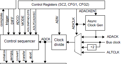
- Is fADCK (ADC conversion clock frequency) referring to the ADC clock source before it is being divided down? I'm assuming its after. But if so, doesn't the "Typical conversion time" example in 23.5.4.6.2 not meet the minimum since 8 MHz/8 = 1 MHz?
Is fADCK (ADC conversion clock frequency) referring to the ADC clock source before it is being divided down? I'm assuming its after. But if so, doesn't the "Typical conversion time" example in 23.5.4.6.2 not meet the minimum since 8 MHz/8 = 1 MHz?
Is fADCK (ADC conversion clock frequency) referring to the ADC clock source before it is being divided down? I'm assuming its after. But if so, doesn't the "Typical conversion time" example in 23.5.4.6.2 not meet the minimum since 8 MHz/8 = 1 MHz?
06-15-2018
08:24 AM
1,059 次查看
Document Number: KL17P64M48SF6RM
16 bit SE output mode
3 回复数
06-20-2018
08:39 AM
776 次查看
NXP Employee
Hello Aaron.
ADCK signal is taken after the clock divider module as shown below:
The complete block diagram is in 23.2.2
I think the example 23.5.4.6.2 it's wrong, the total conversion time it's:
ConversionTime = SFCAdder+AverageNum(BCT+LSTAdder+HSCAdder)
ConversionTime = (3ADCK+5BusK)+32(34ADCK+20ADCK)
ConversionTime = (3/1MHz +5/8MHz)+32(54/1MHz)
ConversionTime =1.731ms
Regards.
06-20-2018
02:52 PM
776 次查看
NXP Employee
Hi Aaron.
Unfortunately seems 23.5.4.6.2 example it's only for explanation purpose and does not considerate real operating conditions for the module. If you followed 23.5.4.6.2 configuration, an unexpected behavior would happen.
Regards.

