- NXP Forums
- Product Forums
- General Purpose MicrocontrollersGeneral Purpose Microcontrollers
- i.MX Forumsi.MX Forums
- QorIQ Processing PlatformsQorIQ Processing Platforms
- Identification and SecurityIdentification and Security
- Power ManagementPower Management
- MCX Microcontrollers
- S32G
- S32K
- S32V
- MPC5xxx
- Other NXP Products
- Wireless Connectivity
- S12 / MagniV Microcontrollers
- Powertrain and Electrification Analog Drivers
- Sensors
- Vybrid Processors
- Digital Signal Controllers
- 8-bit Microcontrollers
- ColdFire/68K Microcontrollers and Processors
- PowerQUICC Processors
- OSBDM and TBDML
-
- Solution Forums
- Software Forums
- MCUXpresso Software and ToolsMCUXpresso Software and Tools
- CodeWarriorCodeWarrior
- MQX Software SolutionsMQX Software Solutions
- Model-Based Design Toolbox (MBDT)Model-Based Design Toolbox (MBDT)
- FreeMASTER
- eIQ Machine Learning Software
- Embedded Software and Tools Clinic
- S32 SDK
- S32 Design Studio
- Vigiles
- GUI Guider
- Zephyr Project
- Voice Technology
- Application Software Packs
- Secure Provisioning SDK (SPSDK)
- Processor Expert Software
-
- Topics
- Mobile Robotics - Drones and RoversMobile Robotics - Drones and Rovers
- NXP Training ContentNXP Training Content
- University ProgramsUniversity Programs
- Rapid IoT
- NXP Designs
- SafeAssure-Community
- OSS Security & Maintenance
- Using Our Community
-
- Cloud Lab Forums
-
- Home
- :
- 汎用マイクロコントローラ
- :
- Kinetisマイクロコントローラ
- :
- Re: FRDM-K64F freedom develpment board as a guideline for a new PCB. With this design a 50MHz clock is generated by the RMII Ethernet PHY and routed to the EXTAL0 (pin 50) of the K64 cpu. Of interest, the FRDM-K64F Rev E3 schematics show the XTAL0 output
FRDM-K64F freedom develpment board as a guideline for a new PCB. With this design a 50MHz clock is generated by the RMII Ethernet PHY and routed to the EXTAL0 (pin 50) of the K64 cpu. Of interest, the FRDM-K64F Rev E3 schematics show the XTAL0 output (pi
- RSS フィードを購読する
- トピックを新着としてマーク
- トピックを既読としてマーク
- このトピックを現在のユーザーにフロートします
- ブックマーク
- 購読
- ミュート
- 印刷用ページ
FRDM-K64F freedom develpment board as a guideline for a new PCB. With this design a 50MHz clock is generated by the RMII Ethernet PHY and routed to the EXTAL0 (pin 50) of the K64 cpu. Of interest, the FRDM-K64F Rev E3 schematics show the XTAL0 output (pi
- 新着としてマーク
- ブックマーク
- 購読
- ミュート
- RSS フィードを購読する
- ハイライト
- 印刷
- 不適切なコンテンツを報告
We are using the design for the FRDM-K64F freedom development board as a guideline for a new PCB. With this design a 50MHz clock is generated by the RMII Ethernet PHY and routed to the EXTAL0 (pin 50) of the K64 cpu. Of interest, the FRDM-K64F Rev E3 schematics show the XTAL0 output (pin 51) connected to GND thru a 0-ohm resistor (R74) via XTAL_K64_MAIN. When using an external clock, normally you leave the XTAL output unconnected. Why is this output connected to ground?
Thanks
- 新着としてマーク
- ブックマーク
- 購読
- ミュート
- RSS フィードを購読する
- ハイライト
- 印刷
- 不適切なコンテンツを報告
Hi David OLSEN,
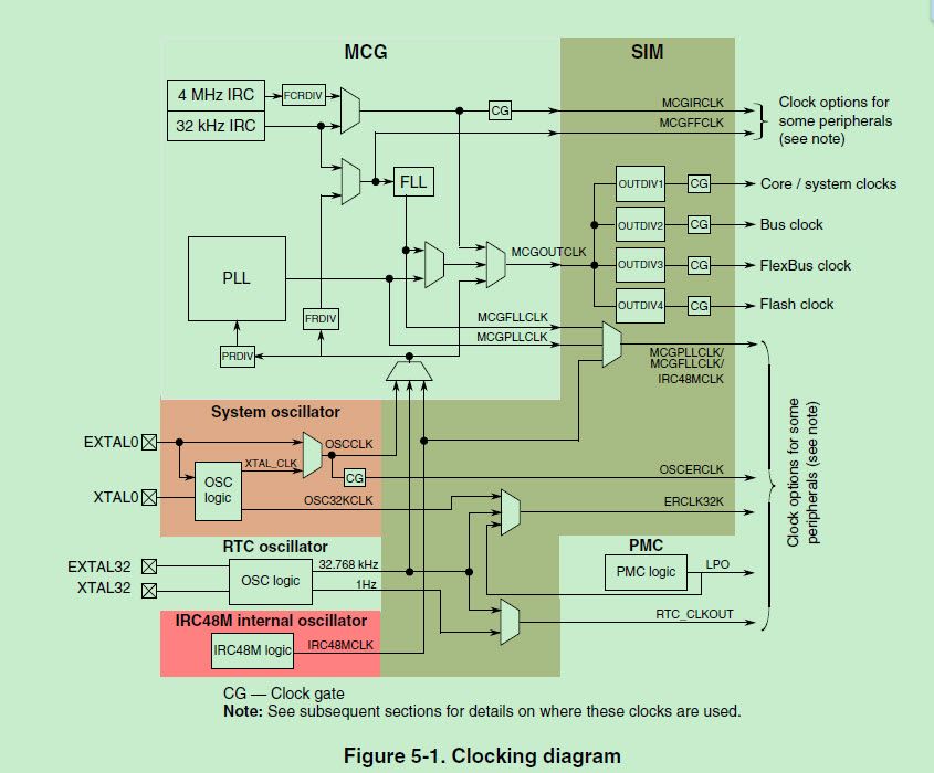
When you use the external reference clock as the clock source, not the external crystal, then you won't use the OSC module, XTAL0 is none used pin, it is better to connect to the ground, just the recommend design.
The clocking diagram can help you to understand it.
Wish it helps you!
If you still have question, please contact me!
Have a great day,
Jingjing
-----------------------------------------------------------------------------------------------------------------------
Note: If this post answers your question, please click the Correct Answer button. Thank you!
-----------------------------------------------------------------------------------------------------------------------
