- Forums
- Product Forums
- General Purpose MicrocontrollersGeneral Purpose Microcontrollers
- i.MX Forumsi.MX Forums
- QorIQ Processing PlatformsQorIQ Processing Platforms
- Identification and SecurityIdentification and Security
- Power ManagementPower Management
- MCX Microcontrollers
- S32G
- S32K
- S32V
- MPC5xxx
- Other NXP Products
- Wireless Connectivity
- S12 / MagniV Microcontrollers
- Powertrain and Electrification Analog Drivers
- Sensors
- Vybrid Processors
- Digital Signal Controllers
- 8-bit Microcontrollers
- ColdFire/68K Microcontrollers and Processors
- PowerQUICC Processors
- OSBDM and TBDML
-
- Solution Forums
- Software Forums
- MCUXpresso Software and ToolsMCUXpresso Software and Tools
- CodeWarriorCodeWarrior
- MQX Software SolutionsMQX Software Solutions
- Model-Based Design Toolbox (MBDT)Model-Based Design Toolbox (MBDT)
- FreeMASTER
- eIQ Machine Learning Software
- Embedded Software and Tools Clinic
- S32 SDK
- S32 Design Studio
- GUI Guider
- Zephyr Project
- Voice Technology
- Application Software Packs
- Secure Provisioning SDK (SPSDK)
- Processor Expert Software
- MCUXpresso Training Hub
-
- Topics
- Mobile Robotics - Drones and RoversMobile Robotics - Drones and Rovers
- NXP Training ContentNXP Training Content
- University ProgramsUniversity Programs
- Rapid IoT
- NXP Designs
- SafeAssure-Community
- OSS Security & Maintenance
- Using Our Community
-
- Cloud Lab Forums
-
- Knowledge Bases
NVT2002
HI NXP team,
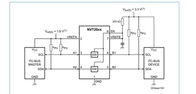
I have to translate the signal from 5V to 1.8V, I have connected the VrefB- 5V and VrefA-1.8V
Question -
Will it make any problem if I connect high-side portion to the I2C master and connect the low-side to I2C device ?
because I see in Application notes and Datasheet information show the low-side portion of the chip to be connected to the I2C master, while the high-side be the I2C device.
Thank you
Hi Pjanek,
no, there is no issue. You can connect I2C master on high side. Please note, that EN is controlled by the Vref(B) logic levels.
With Best Regards,
Jozef
Hello Kozon, I also use the design, which is I2C master(NXP MCU 5V) on VerB, I2C device(3V3) on VerA, but I have one issue, which is as below: when I2C master send the message to the device, I found that the VerB side waveform is normal, but on VerA side, the waveform is distorted , and the high level(3V3) cannot be down to low level(0V) quickly, could you please help me resolve the issue? Thanks a lot!
