- Forums
- Product Forums
- General Purpose MicrocontrollersGeneral Purpose Microcontrollers
- i.MX Forumsi.MX Forums
- QorIQ Processing PlatformsQorIQ Processing Platforms
- Identification and SecurityIdentification and Security
- Power ManagementPower Management
- Wireless ConnectivityWireless Connectivity
- RFID / NFCRFID / NFC
- Advanced AnalogAdvanced Analog
- MCX Microcontrollers
- S32G
- S32K
- S32V
- MPC5xxx
- Other NXP Products
- S12 / MagniV Microcontrollers
- Powertrain and Electrification Analog Drivers
- Sensors
- Vybrid Processors
- Digital Signal Controllers
- 8-bit Microcontrollers
- ColdFire/68K Microcontrollers and Processors
- PowerQUICC Processors
- OSBDM and TBDML
- S32M
- S32Z/E
-
- Solution Forums
- Software Forums
- MCUXpresso Software and ToolsMCUXpresso Software and Tools
- CodeWarriorCodeWarrior
- MQX Software SolutionsMQX Software Solutions
- Model-Based Design Toolbox (MBDT)Model-Based Design Toolbox (MBDT)
- FreeMASTER
- eIQ Machine Learning Software
- Embedded Software and Tools Clinic
- S32 SDK
- S32 Design Studio
- GUI Guider
- Zephyr Project
- Voice Technology
- Application Software Packs
- Secure Provisioning SDK (SPSDK)
- Processor Expert Software
- Generative AI & LLMs
-
- Topics
- Mobile Robotics - Drones and RoversMobile Robotics - Drones and Rovers
- NXP Training ContentNXP Training Content
- University ProgramsUniversity Programs
- Rapid IoT
- NXP Designs
- SafeAssure-Community
- OSS Security & Maintenance
- Using Our Community
-
- Cloud Lab Forums
-
- Knowledge Bases
- ARM Microcontrollers
- i.MX Processors
- Identification and Security
- Model-Based Design Toolbox (MBDT)
- QorIQ Processing Platforms
- S32 Automotive Processing Platform
- Wireless Connectivity
- CodeWarrior
- MCUXpresso Suite of Software and Tools
- MQX Software Solutions
- RFID / NFC
- Advanced Analog
-
- NXP Tech Blogs
- Home
- :
- Product Forums
- :
- Digital Signal Controllers
- :
- 56F82xx I2C0 master bug?
56F82xx I2C0 master bug?
- Subscribe to RSS Feed
- Mark Topic as New
- Mark Topic as Read
- Float this Topic for Current User
- Bookmark
- Subscribe
- Mute
- Printer Friendly Page
56F82xx I2C0 master bug?
- Mark as New
- Bookmark
- Subscribe
- Mute
- Subscribe to RSS Feed
- Permalink
- Report Inappropriate Content
When using I2C1 module in 56F82xx DSC, there is no issue; If using I2C0 module in 56F82xx DSC as master, with EEPROM 24LC02 connected, DSC can get ACK from EEPROM for this byte transfer by sending Device Address (0xA0); while get NACK from EEPROM for second byte by sending any ROM Address.
code segment:
usigned char u8ErrStatus; u8ErrStatus = 0; I2C0_Start(); u8ErrStatus = I2C0_MasterByteWrite(u8DevAddr); u8ErrStatus = I2C0_MasterByteWrite(u8MemAddr); //failed at 9th pulse of clock when sending 2nd byte I2C0_RepeatStart(); u8ErrStatus = I2C0_MasterByteWrite(u8DevAddr | 0x01); u8ErrStatus = I2C0_MasterByteRead(u8Data, I2C0_SEND_NACK); I2C0_Stop();
Appreciated anyone can point out the mistake in above code segment......or, is there any Errata that can explain why I2C1 can but I2C0 can't.
- Mark as New
- Bookmark
- Subscribe
- Mute
- Subscribe to RSS Feed
- Permalink
- Report Inappropriate Content
It should work the same on both I2C0 and I2C1. What may differ is the pin configuration and board layout for the pin.
For I2C, do not drive the pins configured to the bus. Use the mode where the DSC only forces the signal low, and allows the bus to pull up the signals.
In software, make sure that the pins configuration is totally correct. For the hardware, observe the waveforms and determine if the bus meets the specification. The bus includes the external voltage supply pulling up the bus.
- Mark as New
- Bookmark
- Subscribe
- Mute
- Subscribe to RSS Feed
- Permalink
- Report Inappropriate Content
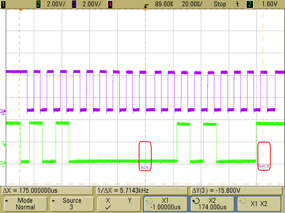
Thanks John's prompt response.. Attached is the waveform that I captured at SCL and SDA signal of I2C0 module.
You can see that ACK can be obtained after master sends Device Address to slave, but NACK will be obtained after master sends any Memory Address (0x28 for example).
I tried to change Device Address rather than 0x5? (? means 0 ~ F), the response can get NACK. So, the configuration should be OK for I2C0 module. Compared with I2C1 configuration, there is no distinct difference on each register respectively.
- Mark as New
- Bookmark
- Subscribe
- Mute
- Subscribe to RSS Feed
- Permalink
- Report Inappropriate Content
Would you be able to cut and jump your board so that the same circuit that works is connected to the i2c pins that seem to be problematic?
How many memory devices are you addressing in your system, and at what addresses?
Perhaps a schematic would be good of the devices on the I2C bus.
- Mark as New
- Bookmark
- Subscribe
- Mute
- Subscribe to RSS Feed
- Permalink
- Report Inappropriate Content
It's inconvenient to rework the board to use I2C1 instead of I2C0 to connect EEPROM for verification. What I had done were:
(1) extract the source code from the good project which work well with I2C1 connecting EEPROM;
(2) build a new project with the extracted source code that also can work well with I2C1 on the same board;
(3) change all the I2C1 to I2C0 to build the above project but it cannot work well with another board where the same type of EEPROM is connected to I2C0 interface.
The waveform is same as the privious reply depicted, in which the 9th clock of 2nd byte will get NACK response.
