- Forums
- Product Forums
- General Purpose MicrocontrollersGeneral Purpose Microcontrollers
- i.MX Forumsi.MX Forums
- QorIQ Processing PlatformsQorIQ Processing Platforms
- Identification and SecurityIdentification and Security
- Power ManagementPower Management
- Wireless ConnectivityWireless Connectivity
- RFID / NFCRFID / NFC
- Advanced AnalogAdvanced Analog
- MCX Microcontrollers
- S32G
- S32K
- S32V
- MPC5xxx
- Other NXP Products
- S12 / MagniV Microcontrollers
- Powertrain and Electrification Analog Drivers
- Sensors
- Vybrid Processors
- Digital Signal Controllers
- 8-bit Microcontrollers
- ColdFire/68K Microcontrollers and Processors
- PowerQUICC Processors
- OSBDM and TBDML
- S32M
- S32Z/E
-
- Solution Forums
- Software Forums
- MCUXpresso Software and ToolsMCUXpresso Software and Tools
- CodeWarriorCodeWarrior
- MQX Software SolutionsMQX Software Solutions
- Model-Based Design Toolbox (MBDT)Model-Based Design Toolbox (MBDT)
- FreeMASTER
- eIQ Machine Learning Software
- Embedded Software and Tools Clinic
- S32 SDK
- S32 Design Studio
- GUI Guider
- Zephyr Project
- Voice Technology
- Application Software Packs
- Secure Provisioning SDK (SPSDK)
- Processor Expert Software
- Generative AI & LLMs
-
- Topics
- Mobile Robotics - Drones and RoversMobile Robotics - Drones and Rovers
- NXP Training ContentNXP Training Content
- University ProgramsUniversity Programs
- Rapid IoT
- NXP Designs
- SafeAssure-Community
- OSS Security & Maintenance
- Using Our Community
-
- Cloud Lab Forums
-
- Knowledge Bases
- ARM Microcontrollers
- i.MX Processors
- Identification and Security
- Model-Based Design Toolbox (MBDT)
- QorIQ Processing Platforms
- S32 Automotive Processing Platform
- Wireless Connectivity
- CodeWarrior
- MCUXpresso Suite of Software and Tools
- MQX Software Solutions
- RFID / NFC
- Advanced Analog
-
- NXP Tech Blogs
- Home
- :
- General Purpose Microcontrollers
- :
- Kinetis Microcontrollers
- :
- Micro MKM34Z256VLL7 damages
Micro MKM34Z256VLL7 damages
- Subscribe to RSS Feed
- Mark Topic as New
- Mark Topic as Read
- Float this Topic for Current User
- Bookmark
- Subscribe
- Mute
- Printer Friendly Page
Micro MKM34Z256VLL7 damages
- Mark as New
- Bookmark
- Subscribe
- Mute
- Subscribe to RSS Feed
- Permalink
- Report Inappropriate Content
Hello,
I am using MKM34Z256VLL7 controller in my application. During development I stuck up in one critical issue i.e., Micro controller damage and also it is not able to reprogram.
While scrutinizing the issue, I found that if I connect - disconnect the Micro UART connection (Pin 91 and Pin 92) to external communication devices then micros are getting damaged; UART is running on 3.3V supply/signal level.
Another in recent experience, Micro damaged just while connecting the DSO - oscilloscope probe ground to micro ground. I checked the oscilloscope, its ground was isolated to mains supply and board remains untouched so there is no electrical over stress. Here Micro controller supply remains 3.3V but reset signal is permanently remains at low 0V level. Also I am not able to reprogram it.
Can you please help me to get rid out of this critical issues.
- Mark as New
- Bookmark
- Subscribe
- Mute
- Subscribe to RSS Feed
- Permalink
- Report Inappropriate Content
Hi,
Please refer below thread and try to unlock the KM34 chip.
https://community.nxp.com/thread/439921?commentID=857127#comment-857127
Wish it helps.
Have a great day,
Mike
-----------------------------------------------------------------------------------------------------------------------
Note: If this post answers your question, please click the Correct Answer button. Thank you!
-----------------------------------------------------------------------------------------------------------------------
- Mark as New
- Bookmark
- Subscribe
- Mute
- Subscribe to RSS Feed
- Permalink
- Report Inappropriate Content
Hi Hui_Ma
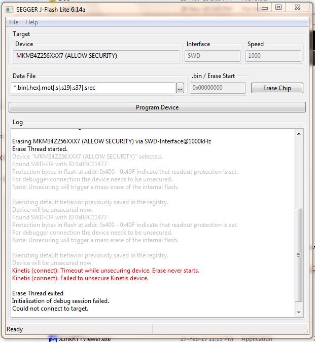
I am getting message "cannot connect to target".
I have tried using J link.exe and J flash tool. Please help me.
Regards
Kalpesh
- Mark as New
- Bookmark
- Subscribe
- Mute
- Subscribe to RSS Feed
- Permalink
- Report Inappropriate Content
Hi Kalpesh,
Could you post the KM34 debug interface schematics for double check?
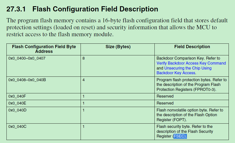
And please provide the Flash configuration Field Value also.
Have a great day,
Mike
-----------------------------------------------------------------------------------------------------------------------
Note: If this post answers your question, please click the Correct Answer button. Thank you!
-----------------------------------------------------------------------------------------------------------------------
- Mark as New
- Bookmark
- Subscribe
- Mute
- Subscribe to RSS Feed
- Permalink
- Report Inappropriate Content
Here, I am not able to upload interface for Debug image.
Message comes "You are not allowed to create or update this content"
BTW,
FSEC value : 0xFE
Debug interface through SWD :
Pins of micro controllers interface as below;
pin 56 : Reset having external RC delay (10 kohm & 10nF ceramic chip capacitor)
pin 65 : Debug IO
pin 66 : Debug Clock
Vdd & Ground
I am using J link debugger from Segger.
With above interface I am able to program and debug other micro controllers which are functionally ok (not locked/damaged) and thereby I believe interface is ok, any feedback please.
My problem is getting severe and development stuck up.
Another points I want to clarify that, in my design TAMPER0, TAMPER1 & TAMPER2 are grounded and I have made ND logic disabled in bootloader. Also in my design there is no RTC battery and RTC is disabled in application. Any feedback please?
Regards
Kalpesh
- Mark as New
- Bookmark
- Subscribe
- Mute
- Subscribe to RSS Feed
- Permalink
- Report Inappropriate Content
Hi,
The FSEC value 0xFE means KM34 is unsecured and debugger isn't blocked.
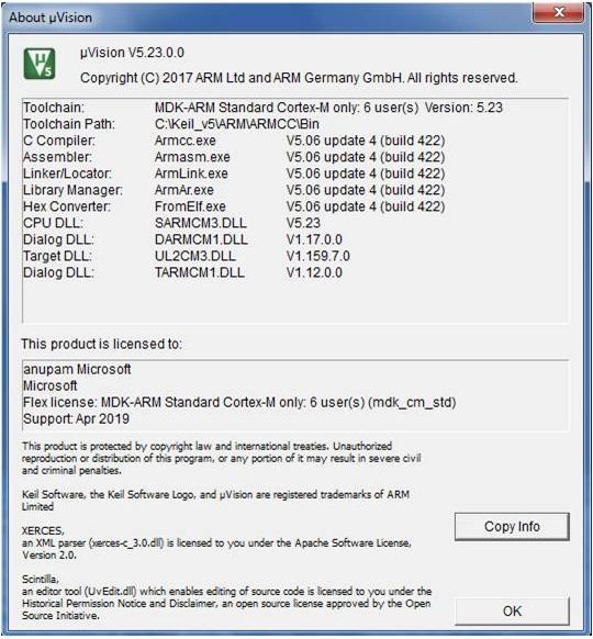
You mentioned debug the code, so which IDE software are you using?
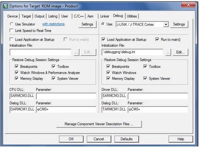
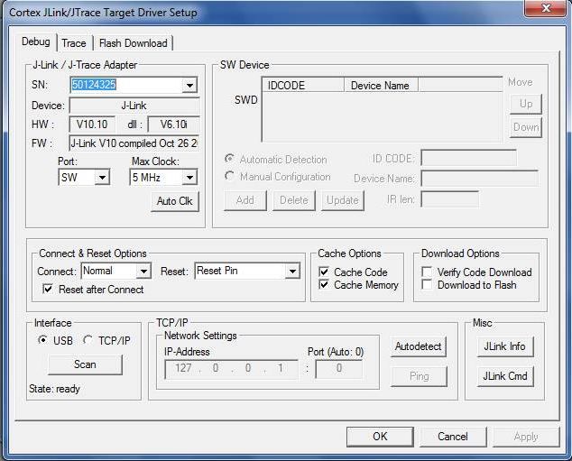
Could you post your IDE debugger panel setting for double check? Thanks.
Have a great day,
Mike
-----------------------------------------------------------------------------------------------------------------------
Note: If this post answers your question, please click the Correct Answer button. Thank you!
-----------------------------------------------------------------------------------------------------------------------
- Mark as New
- Bookmark
- Subscribe
- Mute
- Subscribe to RSS Feed
- Permalink
- Report Inappropriate Content
Hello Mike,
I am using Keil V5.23 and debugger settings snapshots are attached here.
I have analyzed and found,
In some of units I able to unlock the Micro controller but just next if I connect the board to J link debugger to reprogram, it shows the message “cannot connect to target”.
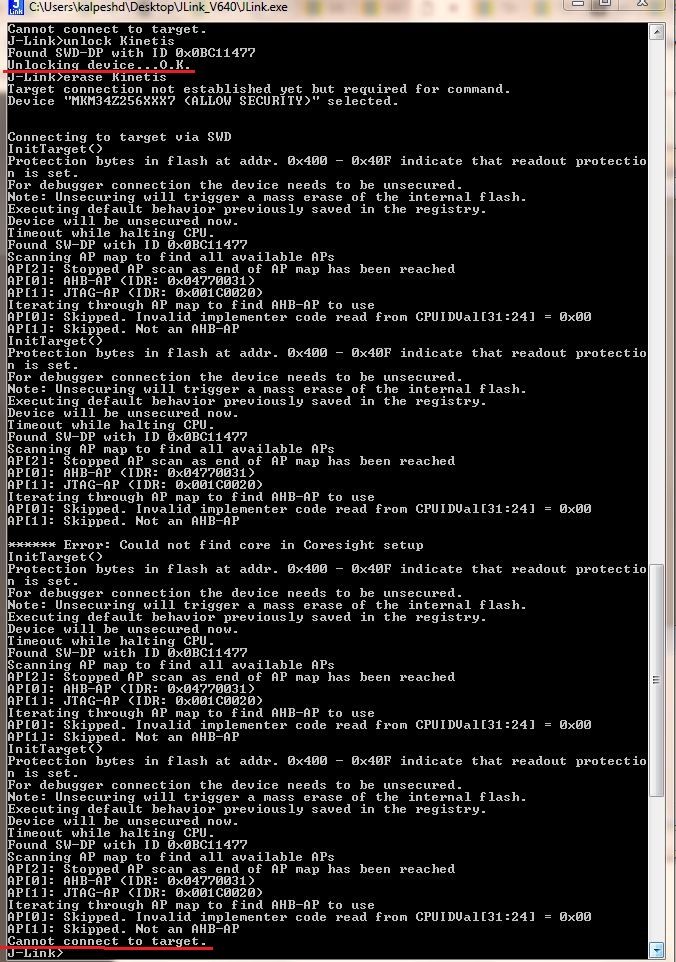
Later I think to erase the chip using “erase Kinetis” command through jlink.exe (command window) but it shows timeout while halting the CPU and couldn’t connect to target. If you can interpret the logs then we can solve the problem. For reference I have attached “Unlock OK_Erase Not OK.jpg” here in attachment.
Please give your feedback..
Regards
Kalpesh Dodiya
- Mark as New
- Bookmark
- Subscribe
- Mute
- Subscribe to RSS Feed
- Permalink
- Report Inappropriate Content
Hi,
Please try with attached J-Link script.
The Kinetis Kxx Cortex-M4 erase all and unsecure manual in Chinese, I add the translation for your reference.
I think this J-Link script also be suitable for ARM Cortex-M0+ core.
Wish it helps.
Have a great day,
Mike
-----------------------------------------------------------------------------------------------------------------------
Note: If this post answers your question, please click the Correct Answer button. Thank you!
-----------------------------------------------------------------------------------------------------------------------
