- Forums
- Product Forums
- General Purpose MicrocontrollersGeneral Purpose Microcontrollers
- i.MX Forumsi.MX Forums
- QorIQ Processing PlatformsQorIQ Processing Platforms
- Identification and SecurityIdentification and Security
- Power ManagementPower Management
- Wireless ConnectivityWireless Connectivity
- RFID / NFCRFID / NFC
- Advanced AnalogAdvanced Analog
- MCX Microcontrollers
- S32G
- S32K
- S32V
- MPC5xxx
- Other NXP Products
- S12 / MagniV Microcontrollers
- Powertrain and Electrification Analog Drivers
- Sensors
- Vybrid Processors
- Digital Signal Controllers
- 8-bit Microcontrollers
- ColdFire/68K Microcontrollers and Processors
- PowerQUICC Processors
- OSBDM and TBDML
- S32M
- S32Z/E
-
- Solution Forums
- Software Forums
- MCUXpresso Software and ToolsMCUXpresso Software and Tools
- CodeWarriorCodeWarrior
- MQX Software SolutionsMQX Software Solutions
- Model-Based Design Toolbox (MBDT)Model-Based Design Toolbox (MBDT)
- FreeMASTER
- eIQ Machine Learning Software
- Embedded Software and Tools Clinic
- S32 SDK
- S32 Design Studio
- GUI Guider
- Zephyr Project
- Voice Technology
- Application Software Packs
- Secure Provisioning SDK (SPSDK)
- Processor Expert Software
- Generative AI & LLMs
-
- Topics
- Mobile Robotics - Drones and RoversMobile Robotics - Drones and Rovers
- NXP Training ContentNXP Training Content
- University ProgramsUniversity Programs
- Rapid IoT
- NXP Designs
- SafeAssure-Community
- OSS Security & Maintenance
- Using Our Community
-
- Cloud Lab Forums
-
- Knowledge Bases
- ARM Microcontrollers
- i.MX Processors
- Identification and Security
- Model-Based Design Toolbox (MBDT)
- QorIQ Processing Platforms
- S32 Automotive Processing Platform
- Wireless Connectivity
- CodeWarrior
- MCUXpresso Suite of Software and Tools
- MQX Software Solutions
- RFID / NFC
- Advanced Analog
-
- NXP Tech Blogs
- Home
- :
- ARM Microcontrollers
- :
- Kinetis Microcontrollers Knowledge Base
- :
- External flash control via kinetis M series SPI module
External flash control via kinetis M series SPI module
- Subscribe to RSS Feed
- Mark as New
- Mark as Read
- Bookmark
- Subscribe
- Printer Friendly Page
- Report Inappropriate Content
External flash control via kinetis M series SPI module
External flash control via kinetis M series SPI module
- Abstract
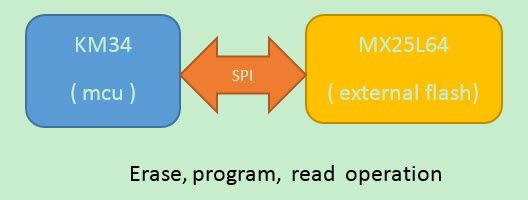
Kinetis M series MCU is Freescale’s Metrology microcontrollers based on ARM Cortex M0+ cores. The SPI module of KM provides for full-duplex, synchronous, serial communication between the MCU and peripheral devices, it also has programmable 8 or 16 bit data transmission length, 64bit FIFO mode for data transfers, DMA transmit and receive features, single wire bidirectional mode, etc. This document is mainly use the KM34Z256VLQ7 SPI module realize the erase, program and read operation in external flash MX25L6404EM2I, it also gives sample code of the detail command external flash operation, and at last, print the testing code via UART.
1.SPI pin assignment and basic code
(1) SPI pin assignment
SPI signal | Pin name | Description |
SPI_SS | PTD1 | Slave select |
SPI_SCK | PTD2 | SPI serial clock |
SPI_MOSI | PTD3 | Master data out, slave data in |
SPI_MISO | PTD4 | Master data in, slave data out |
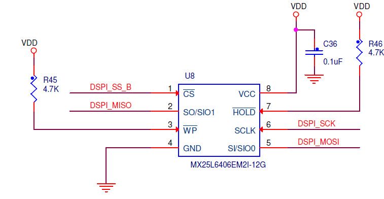
External flash MX25L6404EM2I circuit:
(2) SPI initialization
SPI initialization configuration the SPI pin, SPI module baud, master or slave mode, module enable, etc. the code just as following:
SIM_SCGC4 |= SIM_SCGC4_SPI0_MASK|SIM_SCGC4_SPI1_MASK;
SIM_SCGC5 |= SIM_SCGC5_PORTD_MASK;
void serial_flash_init(void)
{

    PORTD_PCR1 &= ~PORT_PCR_MUX_MASK;
    PORTD_PCR1 |= PORT_PCR_MUX(1) |0X03;                                           //Use PTD1 as SPI0_SS  // configure it as the GPIO
    PORTD_PCR2 &= ~PORT_PCR_MUX_MASK;
    PORTD_PCR2 |= PORT_PCR_MUX(3) |0X03;                                           //Use PTD2 as SPI0_SCK
    PORTD_PCR3 &= ~PORT_PCR_MUX_MASK;
    PORTD_PCR3 |= PORT_PCR_MUX(3) |0X03;                                           //Use PTD3 as SPI0_MOSI
    PORTD_PCR4 &= ~PORT_PCR_MUX_MASK;
    PORTD_PCR4 = PORT_PCR_MUX(3) |0X03;                                            //Use PTD4 as SPI0_MISO

    GPIOD_PDDR |=  0X02; // SS pin output
    GPIOD_PDOR |=  0X02; //  SS pin high


    SPI0_C1 |= SPI_C1_MSTR_MASK; // SPI0 master mode

    SPI0_BR = 0x43;  //SPPR = 4, SPR = 3, bps div = (SPPR+1)*2^(SPR+1) = 80, baudrate= 24Mhz/80=300khz
    SPI0_C1 |= SPI_C1_SSOE_MASK;
    SPI0_C1 &= (~SPI_C1_CPHA_MASK);  // clock polarity
    SPI0_C1 &= (~SPI_C1_CPOL_MASK);  //clock phase
    SPI0_C1 &= (~SPI_C1_LSBFE_MASK);  // LSB:most significant

    SPI0_C1 &= (~SPI_C1_SPIE_MASK);                  //Disable RX interrrupt
    SPI0_C1 &= (~SPI_C1_SPTIE_MASK);         //Disable the transmit interrupt
    SPI0_C2 |= SPI_C2_MODFEN_MASK;

    SPI0_C1 |= SPI_C1_SPE_MASK;  // enable SPI module
}
(3) One byte transfer code
uint8 hal_spi_transfer_one_byte(uint8 v)
{
   int dummy =0;
   char buff=0;

   while ((SPI0_S & SPI_S_SPTEF_MASK) == 0)  // wait for transmit buffer empty
   {
                dummy++;
    }
   dummy = SPI0_S;
   SPI0_DL = v;   // send one byte to transmit buffer

   while ((SPI0_S & SPI_S_SPRF_MASK) == 0); // wait ready buffer full
   buff = SPI0_DL;  // read one received byte
   return buff;         // return the received byte


  }
3 Code realization for external flash operation command
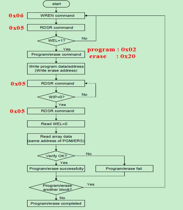
At first, refer to the external flash program / erase flow, then I will give the according command code realization one by one.
Take flash sector erase flow as an example, the according code is :
void hal_spi_dev_flash_erase_sector(uint8 addr)
{
 write_enable();      // WREN command
 spi_wait(WEL);     // RDSR command and wait WEL=1
 hal_spi_transfe_start();    // enable CS pin , CS=0
 hal_spi_transfer_one_byte(CMD_SECTOR_ERASE);   // erase one sector (4KByte)command
 hal_spi_transfer_one_byte(addr>>16);  // address
 hal_spi_transfer_one_byte(addr>>8);
 hal_spi_transfer_one_byte(addr>>0);
 hal_spi_transfe_stop();  // disable CS pin, CS=1
 spi_wait(WIP);    // RDSR command and wait WIP=0;


  }
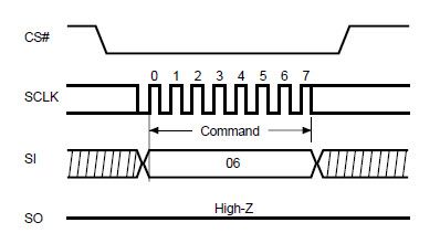
(1)Write enable (WREN) command : 0X06
static void write_enable(void)
{
    hal_spi_transfe_start();  // enable CS pin , CS=0
    hal_spi_transfer_one_byte(CMD_WRITE_EN);  // Send WREN command
    hal_spi_transfe_stop();  // disable CS pin, CS=1


  }
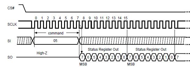
(2)Read status register (RDSR) sequence: 0X05
static void spi_wait(uint8 CMD)
{
 if(CMD == WEL)
 while(get_sr()&0x02 != 0x02); // wait until WEL bit =1
 else if(CMD == WIP)
 while(get_sr()&0x01 != 0x00); // wait until WIP bit =0
}

static uint8 get_sr(void)
{
    uint8 v;
    hal_spi_transfe_start(); // enable CS pin , CS=0
    hal_spi_transfer_one_byte(CMD_GET_SR);  // Send RDSR command
    v = hal_spi_transfer_one_byte(0x00); // read states register data
    hal_spi_transfe_stop();    // disable CS pin, CS=1
    return v;


  }
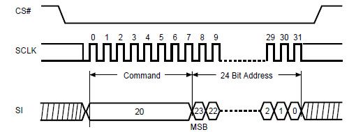
(3) Sector erase (SE) sequence: 0X20
 hal_spi_transfe_start();    // enable CS pin , CS=0
 hal_spi_transfer_one_byte(CMD_SECTOR_ERASE);   // erase one sector (4KByte)command
 hal_spi_transfer_one_byte(addr>>16);  // address
 hal_spi_transfer_one_byte(addr>>8);
 hal_spi_transfer_one_byte(addr>>0);


   hal_spi_transfe_stop();  // disable CS pin, CS=1
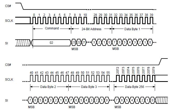
(4) Page program (PP) sequence : 0x02
#define PAGE_SIZE 256

    hal_spi_transfe_start();// enable CS pin , CS=0
 hal_spi_transfer_one_byte(CMD_PROGRAM); //send flash program command
 hal_spi_transfer_one_byte(addr>>16); // flash page base address
 hal_spi_transfer_one_byte(addr>>8);
 hal_spi_transfer_one_byte(addr>>0);
 for(i=0;i<(PAGE_SIZE-1);i++) // send program data to the flash page
 hal_spi_transfer_one_byte(buf[i]);
 hal_spi_transfer_one_byte(buf[i]);


   hal_spi_transfe_stop();// disable CS pin, CS=1
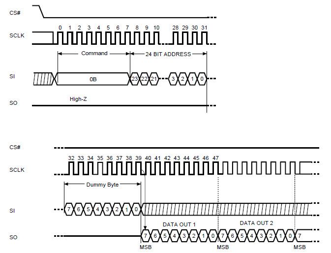
(5) Read at higher Speed(FAST_READ) Sequence: 0X0B
void hal_spi_dev_flash_read_page(uint8 addr, char *buf)
{
 int i;
 hal_spi_transfe_start();  // enable CS pin , CS=0
 hal_spi_transfer_one_byte(CMD_READ); // read command
 hal_spi_transfer_one_byte(addr>>16);  // base address
 hal_spi_transfer_one_byte(addr>>8);
 hal_spi_transfer_one_byte(addr>>0);
 hal_spi_transfer_one_byte(0x00); // dummy byte
 for(i=0;i<(PAGE_SIZE-1);i++)    // read data back from the flash
 buf[i] = hal_spi_transfer_one_byte(0x00);
 buf[i] = hal_spi_transfer_one_byte(0x00);
 hal_spi_transfe_stop();  // disable CS pin, CS=1


  }
4 Experimental result
The test code function is to realize one sector (4KB) erasing, then read one page (256Byte) and print it out, after that, program one page , read and print it out to check the data.
(1)The main function code is :
static char buf[256];
 int i;
 serial_flash_init();  // SPI initialization
 hal_spi_dev_flash_erase_sector(0); // erase one sector(4KByte)
 printf("reading page...\n");
 hal_spi_dev_flash_read_page(0,buf); // read one page(256Byte)
 print_buf(buf,PAGE_SIZE);  // print the read data out

 printf("programing a page...\n");
 for(i=0;i<256;i++)
 buf[i] = i;     // define the data which will write to the flash
 hal_spi_dev_flash_program_page(0,buf); // write 256BYTE to the flash page0

 printf("clearing buffer..\n");
 for(i=0;i<256;i++)    // clear buff
 buf[i] = 0;

 printf("reading page...\n");
 hal_spi_dev_flash_read_page(0,buf); // read the page0 data out
 print_buf(buf,PAGE_SIZE);  // print the read data out


   printf("demo end.\n");
(2) print test data
reading page...
0xFF,0xFF,0xFF,0xFF, 0xFF,0xFF,0xFF,0xFF,
0xFF,0xFF,0xFF,0xFF, 0xFF,0xFF,0xFF,0xFF,
0xFF,0xFF,0xFF,0xFF, 0xFF,0xFF,0xFF,0xFF,
0xFF,0xFF,0xFF,0xFF, 0xFF,0xFF,0xFF,0xFF,
0xFF,0xFF,0xFF,0xFF, 0xFF,0xFF,0xFF,0xFF,
0xFF,0xFF,0xFF,0xFF, 0xFF,0xFF,0xFF,0xFF,
0xFF,0xFF,0xFF,0xFF, 0xFF,0xFF,0xFF,0xFF,
0xFF,0xFF,0xFF,0xFF, 0xFF,0xFF,0xFF,0xFF,
0xFF,0xFF,0xFF,0xFF, 0xFF,0xFF,0xFF,0xFF,
0xFF,0xFF,0xFF,0xFF, 0xFF,0xFF,0xFF,0xFF,
0xFF,0xFF,0xFF,0xFF, 0xFF,0xFF,0xFF,0xFF,
0xFF,0xFF,0xFF,0xFF, 0xFF,0xFF,0xFF,0xFF,
0xFF,0xFF,0xFF,0xFF, 0xFF,0xFF,0xFF,0xFF,
0xFF,0xFF,0xFF,0xFF, 0xFF,0xFF,0xFF,0xFF,
0xFF,0xFF,0xFF,0xFF, 0xFF,0xFF,0xFF,0xFF,
0xFF,0xFF,0xFF,0xFF, 0xFF,0xFF,0xFF,0xFF,
0xFF,0xFF,0xFF,0xFF, 0xFF,0xFF,0xFF,0xFF,
0xFF,0xFF,0xFF,0xFF, 0xFF,0xFF,0xFF,0xFF,
0xFF,0xFF,0xFF,0xFF, 0xFF,0xFF,0xFF,0xFF,
0xFF,0xFF,0xFF,0xFF, 0xFF,0xFF,0xFF,0xFF,
0xFF,0xFF,0xFF,0xFF, 0xFF,0xFF,0xFF,0xFF,
0xFF,0xFF,0xFF,0xFF, 0xFF,0xFF,0xFF,0xFF,
0xFF,0xFF,0xFF,0xFF, 0xFF,0xFF,0xFF,0xFF,
0xFF,0xFF,0xFF,0xFF, 0xFF,0xFF,0xFF,0xFF,
0xFF,0xFF,0xFF,0xFF, 0xFF,0xFF,0xFF,0xFF,
0xFF,0xFF,0xFF,0xFF, 0xFF,0xFF,0xFF,0xFF,
0xFF,0xFF,0xFF,0xFF, 0xFF,0xFF,0xFF,0xFF,
0xFF,0xFF,0xFF,0xFF, 0xFF,0xFF,0xFF,0xFF,
0xFF,0xFF,0xFF,0xFF, 0xFF,0xFF,0xFF,0xFF,
0xFF,0xFF,0xFF,0xFF, 0xFF,0xFF,0xFF,0xFF,
0xFF,0xFF,0xFF,0xFF, 0xFF,0xFF,0xFF,0xFF,
0xFF,0xFF,0xFF,0xFF, 0xFF,0xFF,0xFF,0xFF,
programing a page...
clearing buffer..
reading page...
0x0,0x1,0x2,0x3, 0x4,0x5,0x6,0x7,
0x8,0x9,0xA,0xB, 0xC,0xD,0xE,0xF,
0x10,0x11,0x12,0x13, 0x14,0x15,0x16,0x17,
0x18,0x19,0x1A,0x1B, 0x1C,0x1D,0x1E,0x1F,
0x20,0x21,0x22,0x23, 0x24,0x25,0x26,0x27,
0x28,0x29,0x2A,0x2B, 0x2C,0x2D,0x2E,0x2F,
0x30,0x31,0x32,0x33, 0x34,0x35,0x36,0x37,
0x38,0x39,0x3A,0x3B, 0x3C,0x3D,0x3E,0x3F,
0x40,0x41,0x42,0x43, 0x44,0x45,0x46,0x47,
0x48,0x49,0x4A,0x4B, 0x4C,0x4D,0x4E,0x4F,
0x50,0x51,0x52,0x53, 0x54,0x55,0x56,0x57,
0x58,0x59,0x5A,0x5B, 0x5C,0x5D,0x5E,0x5F,
0x60,0x61,0x62,0x63, 0x64,0x65,0x66,0x67,
0x68,0x69,0x6A,0x6B, 0x6C,0x6D,0x6E,0x6F,
0x70,0x71,0x72,0x73, 0x74,0x75,0x76,0x77,
0x78,0x79,0x7A,0x7B, 0x7C,0x7D,0x7E,0x7F,
0x80,0x81,0x82,0x83, 0x84,0x85,0x86,0x87,
0x88,0x89,0x8A,0x8B, 0x8C,0x8D,0x8E,0x8F,
0x90,0x91,0x92,0x93, 0x94,0x95,0x96,0x97,
0x98,0x99,0x9A,0x9B, 0x9C,0x9D,0x9E,0x9F,
0xA0,0xA1,0xA2,0xA3, 0xA4,0xA5,0xA6,0xA7,
0xA8,0xA9,0xAA,0xAB, 0xAC,0xAD,0xAE,0xAF,
0xB0,0xB1,0xB2,0xB3, 0xB4,0xB5,0xB6,0xB7,
0xB8,0xB9,0xBA,0xBB, 0xBC,0xBD,0xBE,0xBF,
0xC0,0xC1,0xC2,0xC3, 0xC4,0xC5,0xC6,0xC7,
0xC8,0xC9,0xCA,0xCB, 0xCC,0xCD,0xCE,0xCF,
0xD0,0xD1,0xD2,0xD3, 0xD4,0xD5,0xD6,0xD7,
0xD8,0xD9,0xDA,0xDB, 0xDC,0xDD,0xDE,0xDF,
0xE0,0xE1,0xE2,0xE3, 0xE4,0xE5,0xE6,0xE7,
0xE8,0xE9,0xEA,0xEB, 0xEC,0xED,0xEE,0xEF,
0xF0,0xF1,0xF2,0xF3, 0xF4,0xF5,0xF6,0xF7,
0xF8,0xF9,0xFA,0xFB, 0xFC,0xFD,0xFE,0xFF,
demo end
From the print data, we can find the code can realize flash sector erasing , flash program and flash data read out, and the test result is correct.
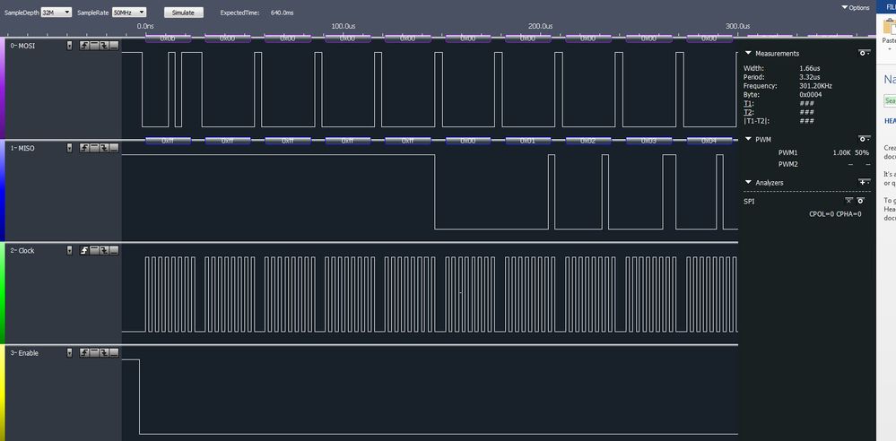
The following wave is the page read data out after flash page program.
The attachment is the testing code.
