- NXP Forums
- Product Forums
- General Purpose MicrocontrollersGeneral Purpose Microcontrollers
- i.MX Forumsi.MX Forums
- QorIQ Processing PlatformsQorIQ Processing Platforms
- Identification and SecurityIdentification and Security
- Power ManagementPower Management
- MCX Microcontrollers
- S32G
- S32K
- S32V
- MPC5xxx
- Other NXP Products
- Wireless Connectivity
- S12 / MagniV Microcontrollers
- Powertrain and Electrification Analog Drivers
- Sensors
- Vybrid Processors
- Digital Signal Controllers
- 8-bit Microcontrollers
- ColdFire/68K Microcontrollers and Processors
- PowerQUICC Processors
- OSBDM and TBDML
-
- Solution Forums
- Software Forums
- MCUXpresso Software and ToolsMCUXpresso Software and Tools
- CodeWarriorCodeWarrior
- MQX Software SolutionsMQX Software Solutions
- Model-Based Design Toolbox (MBDT)Model-Based Design Toolbox (MBDT)
- FreeMASTER
- eIQ Machine Learning Software
- Embedded Software and Tools Clinic
- S32 SDK
- S32 Design Studio
- Vigiles
- GUI Guider
- Zephyr Project
- Voice Technology
- Application Software Packs
- Secure Provisioning SDK (SPSDK)
- Processor Expert Software
-
- Topics
- Mobile Robotics - Drones and RoversMobile Robotics - Drones and Rovers
- NXP Training ContentNXP Training Content
- University ProgramsUniversity Programs
- Rapid IoT
- NXP Designs
- SafeAssure-Community
- OSS Security & Maintenance
- Using Our Community
-
- Cloud Lab Forums
-
- Home
- :
- i.MX Forums
- :
- i.MX RT
- :
- i.MX RT1060 EVKB get pps output from ptp timer
i.MX RT1060 EVKB get pps output from ptp timer
- Subscribe to RSS Feed
- Mark Topic as New
- Mark Topic as Read
- Float this Topic for Current User
- Bookmark
- Subscribe
- Mute
- Printer Friendly Page
- Mark as New
- Bookmark
- Subscribe
- Mute
- Subscribe to RSS Feed
- Permalink
- Report Inappropriate Content
Hi,
I am trying to get pps output from one of the ptp timer channels on RT1060EVKB board, in order to test synchronization accuracy. I tried following Implementing an IEEE 1588 V2 on i.MX RT Using PTPd, FreeRTOS, and lwIP TCP/IP stack (nxp.com), but the code now seems different from the manual. Could you please help me with the changes in the driver?
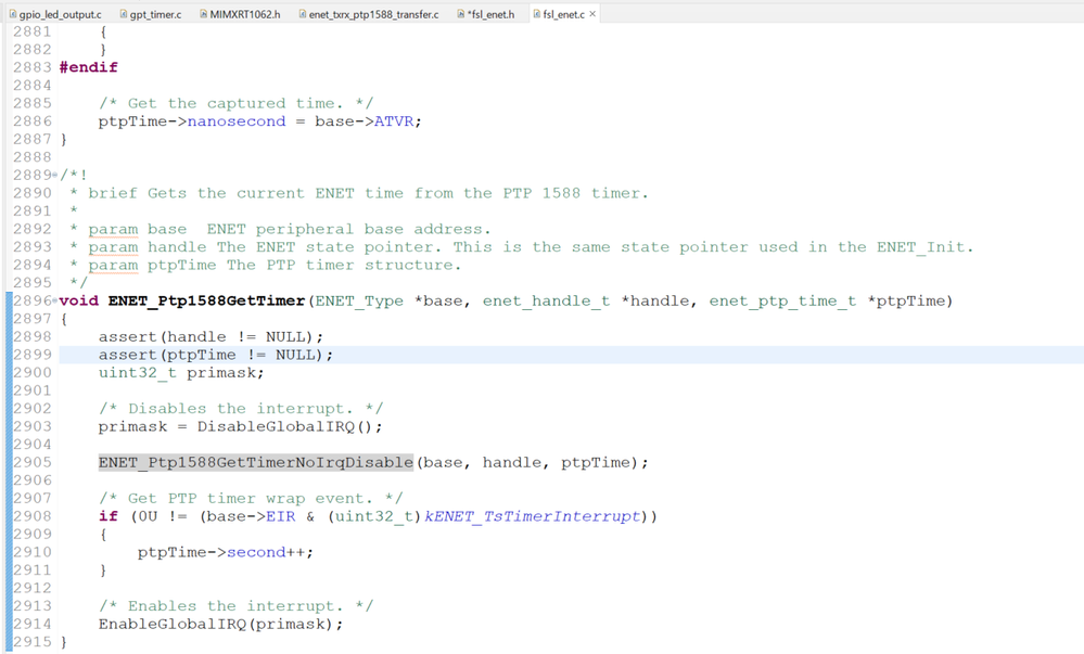
Here is a code snippet:
Moreover, on the EVKB board I have, there is no J22 as the maunal mentioned "As for the i.MX RT1050 and i.MX RT1060 MCUs, the PPS signal is generated directly from the 1588 timer’s channel 3 and configured to output through the GPIO_AD_B1_02 pin. This GPIO signal is routed to the J22-7 pin of the Arduino interface. " What would be the pin for pps output on this board?
Many thanks!
Solved! Go to Solution.
- Mark as New
- Bookmark
- Subscribe
- Mute
- Subscribe to RSS Feed
- Permalink
- Report Inappropriate Content
Hi @Peier ,
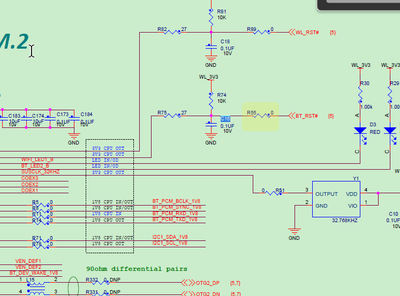
You can remove R55 if you don't want the C16 influence you when you don't use the M.2 interface:
GPIO_AD_B0_07 is also connect to SWD_CLK, JTAG_TCK, so if you also in the debug mode, you can't see it.
I think you still can use GPIO_AD_B1_02 pin, just remove the capacitor.
Wish it helps you!
Best Regards,
Kerry
- Mark as New
- Bookmark
- Subscribe
- Mute
- Subscribe to RSS Feed
- Permalink
- Report Inappropriate Content
Hi @Peier ,
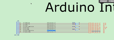
@MultipleMonomials 's reply is correct, to the EVKB, the used RT1062 chip is the same as the EVK board, so you just need to check the pin GPIO_AD_1_02 in the EVKB, it is the J16_7:
Please also note, this pin also connect to the SPDIF_OUT, BT_RST#, CSI_PWDN, you need to make sure the other module is not using this pin, otherwise, you need to remove the related resistor.
Wish it helps you!
If you still have question about it, please kindly let me know.
If your question is solved, please help to mark the correct answer, just to close this case.
Any new issues, welcome to create the new case.
Best Regards,
Kerry
- Mark as New
- Bookmark
- Subscribe
- Mute
- Subscribe to RSS Feed
- Permalink
- Report Inappropriate Content
Hi Kerry,
Thanks for your reply! I have one more question about enabling pps output in the code. In application note "Implementing an IEEE 1588 V2 on i.MX RT Using PTPd", it states "the PPS signal is
generated directly from the 1588 timer’s channel 3 and configured to output through the
GPIO_AD_B1_02 pin". Could you please confirm if it is the same case for the sdk example "evkbmimxrt1060_enet_txrx_ptp1588_transfer" and whether we can change the output pin for pps?
Kind regards,
Peier
- Mark as New
- Bookmark
- Subscribe
- Mute
- Subscribe to RSS Feed
- Permalink
- Report Inappropriate Content
Hi @Peier ,
To the RT1060, it is the same situation.
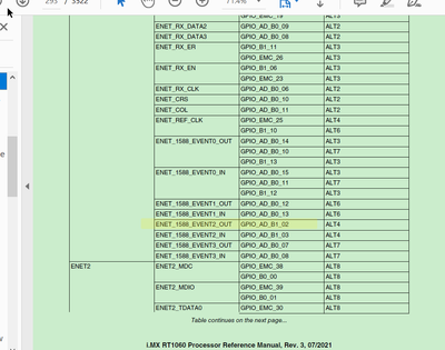
To the channel, you just need to check the 1588 timer output related channel, then configure the related channel:
You can see, also have EVENT1, EENT3 OUT.
Wish it helps you!
Best Regards,
Kerry
- Mark as New
- Bookmark
- Subscribe
- Mute
- Subscribe to RSS Feed
- Permalink
- Report Inappropriate Content
Hi Kerry,
Thanks a lot!
Sorry if this is too specific, but I still cannot see PPS output on pin GPIO_AD_B1_02/J16_7, after making necessary changes in the driver following that application note. I am guessing kENET_PtpTimerChannel3 is the channel to use since interrupts on ENET:1588_EVENT2_OUT are desired. I could not figure out what else was missing - which could be my mistakes.
I saw in the file 'fsl_enet.h' that there is an enum '_enet_ptp_timer_channel_mode' that is not used anywhere. Could you please check if '_enet_ptp_timer_channel_mode' should be used in the code to enable output compare on the desired channel, which is kENET_PtpTimerChannel3?
Kind regards,
Peier
- Mark as New
- Bookmark
- Subscribe
- Mute
- Subscribe to RSS Feed
- Permalink
- Report Inappropriate Content
Hi @Peier ,
About the different channel, in fact, in the previous time, I test it on the RT1170, to the RT106X is the same, you also can refer to it.
This is my related information for the RT1170, you also can refer to it:
- Mark as New
- Bookmark
- Subscribe
- Mute
- Subscribe to RSS Feed
- Permalink
- Report Inappropriate Content
Hi Kerry,
Thanks for your fast reply. I think the problem is with the oscilloscope setting I am using-- it doesn't show the spikes with a very short duration.
In the function ENET_Ptp1588SetChannelOutputPulseWidth, the maximum pulse width is 32 cycles of ptp clock.
* @Param pulseWidth  The pulse width control value, range from 0 ~ 31.
 *                     0  --- pulse width is one 1588 clock cycle.
 *                     31 --- pulse width is thirty two 1588 clock cycles.
1 cycle is 40 ns when the PTP clock frequency is 25 Mhz, so the spike duration is around 1 us - which is almost invisible when the scale is a few seconds. If I zoom in to a few us, I can see a pulse with 1.16V.
So is there a way to increase the pulse width to some ms? And is it possible to change the amplitude to 3.3 V?
Kind regards,
Peier
- Mark as New
- Bookmark
- Subscribe
- Mute
- Subscribe to RSS Feed
- Permalink
- Report Inappropriate Content
Hi @Peier ,
Thanks for your updated information.
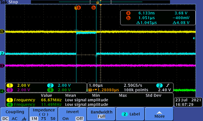
You can use the oscillator to trigger the pulse, then you can get it, in fact, in the previous time, when I test the RT1170 ptp output, I made the same mistake like you, at last, when I use the trigger, I can get the ns puse like this :
In my memory, if you want to get large pulse, you may need to change the time clock source, but that no meaning to you.
If you just want to get the large pulse, I think, you even can use other timer, instead of the ptp timer, right? ptp timer just have the high frequency. You can adjust your oscillatorscope, just to make sure you can capture the puse at first.
Wish it helps you!
If you still have question about it, please kindly let me know.
Best Regards,
Kerry
- Mark as New
- Bookmark
- Subscribe
- Mute
- Subscribe to RSS Feed
- Permalink
- Report Inappropriate Content
Hi Kerry,
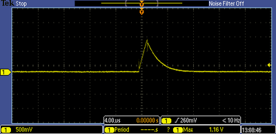
Yes I can observe the pulse on trigger mode. I need pps output from PTP timer specifically, because it is for measuring PTP synchronization accuracy. However, the pulse I see is like this:
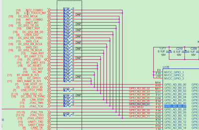
It might be due to large capacitor as @MultipleMonomials mentioned- so I am trying to see if there is other pin I can use. ENET:1588_EVENT3_OUT can be routed to J19_7, so I used channel 4, but I didn't get any output. I checked the schematic and saw this:
Does it mean I need to solder something on the board?
Thanks again!
Kind regards,
Peier
- Mark as New
- Bookmark
- Subscribe
- Mute
- Subscribe to RSS Feed
- Permalink
- Report Inappropriate Content
Hi @Peier ,
You can remove R55 if you don't want the C16 influence you when you don't use the M.2 interface:
GPIO_AD_B0_07 is also connect to SWD_CLK, JTAG_TCK, so if you also in the debug mode, you can't see it.
I think you still can use GPIO_AD_B1_02 pin, just remove the capacitor.
Wish it helps you!
Best Regards,
Kerry
- Mark as New
- Bookmark
- Subscribe
- Mute
- Subscribe to RSS Feed
- Permalink
- Report Inappropriate Content
GPIO_AD_B1_02 is routed to J16-7 on the MIMXRT1060 EVK. However, in my experience using this pin for PPS is a bad idea because it has a large capacitor on it (C16) which prevents it from generating a sharp edge signal.
