- Forums
- Product Forums
- General Purpose MicrocontrollersGeneral Purpose Microcontrollers
- i.MX Forumsi.MX Forums
- QorIQ Processing PlatformsQorIQ Processing Platforms
- Identification and SecurityIdentification and Security
- Power ManagementPower Management
- Wireless ConnectivityWireless Connectivity
- RFID / NFCRFID / NFC
- Advanced AnalogAdvanced Analog
- MCX Microcontrollers
- S32G
- S32K
- S32V
- MPC5xxx
- Other NXP Products
- S12 / MagniV Microcontrollers
- Powertrain and Electrification Analog Drivers
- Sensors
- Vybrid Processors
- Digital Signal Controllers
- 8-bit Microcontrollers
- ColdFire/68K Microcontrollers and Processors
- PowerQUICC Processors
- OSBDM and TBDML
- S32M
- S32Z/E
-
- Solution Forums
- Software Forums
- MCUXpresso Software and ToolsMCUXpresso Software and Tools
- CodeWarriorCodeWarrior
- MQX Software SolutionsMQX Software Solutions
- Model-Based Design Toolbox (MBDT)Model-Based Design Toolbox (MBDT)
- FreeMASTER
- eIQ Machine Learning Software
- Embedded Software and Tools Clinic
- S32 SDK
- S32 Design Studio
- GUI Guider
- Zephyr Project
- Voice Technology
- Application Software Packs
- Secure Provisioning SDK (SPSDK)
- Processor Expert Software
- Generative AI & LLMs
-
- Topics
- Mobile Robotics - Drones and RoversMobile Robotics - Drones and Rovers
- NXP Training ContentNXP Training Content
- University ProgramsUniversity Programs
- Rapid IoT
- NXP Designs
- SafeAssure-Community
- OSS Security & Maintenance
- Using Our Community
-
- Cloud Lab Forums
-
- Knowledge Bases
- ARM Microcontrollers
- i.MX Processors
- Identification and Security
- Model-Based Design Toolbox (MBDT)
- QorIQ Processing Platforms
- S32 Automotive Processing Platform
- Wireless Connectivity
- CodeWarrior
- MCUXpresso Suite of Software and Tools
- MQX Software Solutions
- RFID / NFC
- Advanced Analog
-
- NXP Tech Blogs
- Home
- :
- i.MX Forums
- :
- i.MX Processors
- :
- FlexSPI inserts random frames into write transactions
FlexSPI inserts random frames into write transactions
- Subscribe to RSS Feed
- Mark Topic as New
- Mark Topic as Read
- Float this Topic for Current User
- Bookmark
- Subscribe
- Mute
- Printer Friendly Page
FlexSPI inserts random frames into write transactions
- Mark as New
- Bookmark
- Subscribe
- Mute
- Subscribe to RSS Feed
- Permalink
- Report Inappropriate Content
I'm implementing communication between an IMX8MN6 CM7 core and an FPGA via FlexSPI in octal mode. I'm seeing the problem that a FlexSPI write transaction inserts random frames into the write transaction that are not in any way specified by the LUT entries.
FlexSPI is configured with "SCLK output free-running", but I was also able to see the error without this setting.
Originally I started with this sequence of FlexSPI LUT entries for a write transaction:
    {// Write command is first byte with LSB = 1
     FLEXSPI_LUT_SEQ(
         // Command "write" is one byte with LSB = 1.
         kFLEXSPI_Command_SDR, kFLEXSPI_8PAD, 0x01,

         // The row address is written in octal mode, 2 bytes = 16 bits.
         kFLEXSPI_Command_RADDR_SDR, kFLEXSPI_8PAD, 16),

     FLEXSPI_LUT_SEQ(
         // Write the data in octal mode, the operand is irrelevant.
         kFLEXSPI_Command_WRITE_SDR, kFLEXSPI_8PAD, 0x04,

         // Stop.
         kFLEXSPI_Command_STOP, kFLEXSPI_1PAD, 0)},
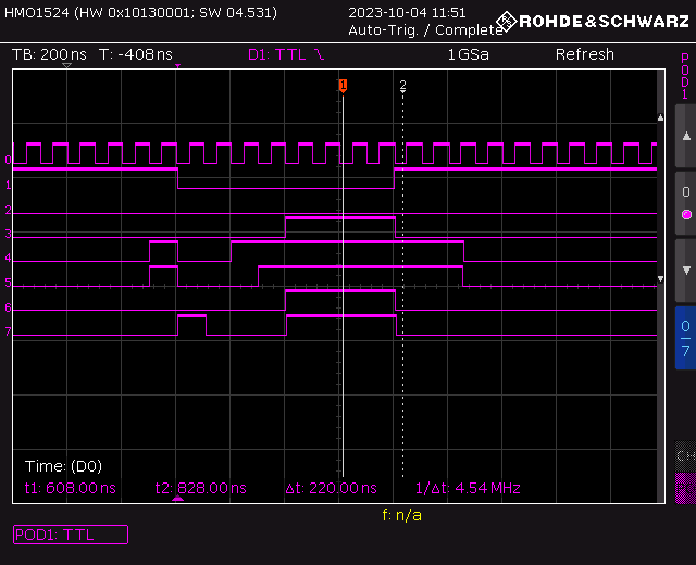
This should result in an SPI transaction that takes seven clock cycles, which it does about half of the times. This is a screen shot from the oscilloscope for a 4-byte write:
The following signals are captured:
| Channel | Description |
| 0 | SPI clock at 10 MHz |
| 1 | SPI chip select |
| 2 | DQS, inactive in write transaction |
| 3-7 | Five least significant bits of the eight SPI data lines |
This is the effect of triggering a FlexSPI write at address 0x08 with a 4-byte data value 0xFFFFFFFF. The signals are as expected:
| SPI clock frame(s) | Value on MOSI lines | Comment |
| 0 | 0x01 | Created by kFLEXSPI_Command_SDR LUT entry with operand 0x01 |
| 1-2 | 0x0008 | Two address bytes 0x0008 created by kFLEXSPI_Command_RADDR_SDR LUT entry with operand 16 |
| 3-6 | 0xFFFFFFFF | Five least significant bits of writing 4-byte value 0xFFFFFFFF with kFLEXSPI_Command_WRITE_SDR LUT entry |
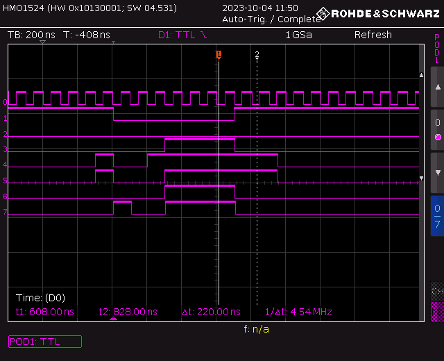
But only roughly half the write transactions look like this. More often the transaction looks like this:
Here we have the following:
| SPI clock frame(s) | Value on MOSI lines | Comment |
| 0 | 0x01 | Correct command 0x01 |
| 1-2 | 0x0008 | Correct address 0x0008 |
| 3 | 0x0C | Incorrect frame that must not be present |
| 4-7 | 0xFFFFFFFF | Correct 4-byte data value 0xFFFFFFFF |
Note that it is reproducible that always the value 0x0C is inserted. I did not see any other value in my tests.
We checked the errata for the IMX8MN6 chip in the NXP document IMX8MN_0N14Y "Mask Set Errata for Mask 0N14Y", and there we found only the following erratum:
ERR050537: FlexSPI: Read timing sequence mismatches with several existing SPI NOR devices in dual, quad, and octal modes
...
In multiple IO modes such as dual, quad, and octal modes, the FlexSPI controller inserts one additional clock cycle following the address (or command modifier) phase in order to prevent contention on bidirectional IO pins.
This does not seem to apply to our situation as we have the problem with a write transaction, but nevertheless we checked whether an additional dummy cycle between the address and the data frames improves the situation. The new LUT for the write transaction looks like this:
    {// Write command is first byte with LSB = 1
     FLEXSPI_LUT_SEQ(
         // Command "write" is one byte with LSB = 1.
         kFLEXSPI_Command_SDR, kFLEXSPI_8PAD, 0x01,

         // The row address is written in octal mode, 2 bytes = 16 bits.
         kFLEXSPI_Command_RADDR_SDR, kFLEXSPI_8PAD, 16),

     FLEXSPI_LUT_SEQ(
        // Dummy cycle as workaround attempt for problem with FlexSPI engine.
        kFLEXSPI_Command_DUMMY_SDR, kFLEXSPI_8PAD, 1,

        // Write the data in octal mode, the operand is irrelevant.
        kFLEXSPI_Command_WRITE_SDR, kFLEXSPI_8PAD, 0x04),

     FLEXSPI_LUT_SEQ(kFLEXSPI_Command_STOP, kFLEXSPI_1PAD, 0, kFLEXSPI_Command_STOP, kFLEXSPI_1PAD, 0)},
This improves the reliability but it does not fix the problem. When running continuous tests the same errors happen on average two or three times after a few ten-thousands of write transactions.
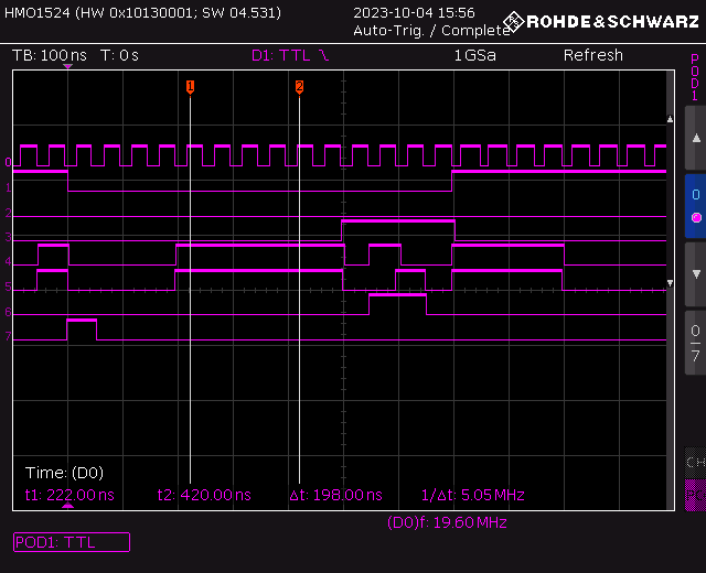
This was with an SPI clock of 10 MHz. We want to reach an SPI clock frequency of 100 MHz. But already with a frequency to 20 MHz the behavior is catastrophic. With the higher clock frequency almost all write transactions are broken, and there are even more extra frames inserted. This is a screen shot from the oscilloscope with an SPI clock frequency of 20 MHz:
With the same LUT table as before the write transaction that should take exactly eight cycles now takes 14 cycles. Now we have this (this screen shot was taken with a different address and data value in the write transaction):
| SPI clock frame(s) | Value on MOSI lines | Comment |
| 0 | 0x01 | Correct command 0x01 |
| 1-2 | two arbitrary address bytes | |
| 3 | dummy cycle | |
| 4-9 | 0x0C | six extra 0x0C bytes |
| 10-13 | four arbitrary data bytes |
This is the FlexSPI deviceconfig structure that we are using:
flexspi_device_config_t deviceconfig = {
    .flexspiRootClk = 10000000, // 10 MHz (D)
    .flashSize            = 1, // 1 kB
    .CSIntervalUnit       = kFLEXSPI_CsIntervalUnit1SckCycle,
    .CSInterval           = 2,
    .CSHoldTime           = 0,
    .CSSetupTime          = 0,
    .dataValidTime        = 0,
    .columnspace          = 0,
    .enableWordAddress    = 0,
    .AWRSeqIndex          = NOR_CMD_LUT_SEQ_IDX_WRITE,
    .AWRSeqNumber         = 1,
    .ARDSeqIndex          = NOR_CMD_LUT_SEQ_IDX_READ,
    .ARDSeqNumber         = 1,
    .AHBWriteWaitUnit     = kFLEXSPI_AhbWriteWaitUnit2AhbCycle,
    .AHBWriteWaitInterval = 0,
};
And this is the FlexSPI initialization code:
    flexspi_config_t config;

    FLEXSPI_GetDefaultConfig(&config);

    config.enableSckFreeRunning = true;

    config.ahbConfig.enableAHBPrefetch    = false;
    config.ahbConfig.enableAHBBufferable  = false;
    config.ahbConfig.enableReadAddressOpt = false;
    config.ahbConfig.enableAHBCachable    = false;

    config.rxSampleClock = kFLEXSPI_ReadSampleClkLoopbackInternally;

    config.enableCombination = true;

    FLEXSPI_Init(base, &config);
What could be causing this unreliable behavior of the FlexSPI peripheral? According to the data sheet FlexSPI should work with SPI clocks up to 66 MHz in SDR mode with internal dummy read strobe and with SPI clocks up to 166 MHz with Flash-provided read strobe.
- Mark as New
- Bookmark
- Subscribe
- Mute
- Subscribe to RSS Feed
- Permalink
- Report Inappropriate Content
Hello @Sanket_Parekh,
thanks for the pointers to the documentation. I think "6.1.5.2.1 FlexSPI Configuration Block" is not relevant for our situation, as we are not booting from a Flash device. We are using FlexSPI to communicate with an FPGA chip.
We think we now found the cause for the extra cycles in the SDK API implementation for FlexSPI writing by IP command.
The "i.MX 8M Nano Applications Processor Reference Manual" says this in "10.2.4.9 Flash access by IP Command":
Flash access could be triggered by IP command in following steps.
• Fill IP TX FIFO with programming data if this is a programing command
(programming flash data, flash status registers etc.)
• Set flash access start address (IPCR0[SFAR]), read/program data size, sequence
index in LUT and sequence number (IPCR1[ISEQNUM]).
• Trigger flash access command by writing 1 to register bit IPCMD[TRG]
• Polling register bit INTR[IPCMDDONE] to wait for this IP command to finish on
FlexSPI interface.And in the subsequent NOTE:
IP TX FIFO could be filled before or after writing IPCR0/
IPCR1/IPCMD register. If SFM command is started with
IP TX FIFO empty, FlexSPI will stop SCLK toggling to
wait for TX data ready automatically.
From our CM7 program we are using the SDK API function "FLEXSPI_TransferBlocking()". This function configures the FlexSPI engine and performs the actual transfer. What it does is to start the FlexSPI transfer before actually filling the IP TX FIFO. See the implementation of FLEXSPI_TransferBlocking() in the MCUXpresso SDK:
    /* Start Transfer. */
    base->IPCMD |= FLEXSPI_IPCMD_TRG_MASK;

    if ((xfer->cmdType == kFLEXSPI_Write) || (xfer->cmdType == kFLEXSPI_Config))
    {
        result = FLEXSPI_WriteBlocking(base, (uint8_t *)xfer->data, xfer->dataSize);
    }
    else if (xfer->cmdType == kFLEXSPI_Read)
    {
        result = FLEXSPI_ReadBlocking(base, (uint8_t *)xfer->data, xfer->dataSize);
    }
    else
    {
        /* Empty else. */
    }
With the write to base->IPCMD the FlexSPI transfer is started, and only in the subsequent call to FLEXSPI_WriteBlocking() the IP TX FIFO is filled with the data to write. If the SPI clock frequency is high enough, the FIFO will not be filled yet when the FlexSPI engine wants to transfer the data, so it inserts the dummy frames, and "SCLK output free-running" is not set it will stop the SPI clock until the IP TX FIFO has been filled with data. The higher the SPI frequency is, the more dummy cycles will be inserted by the FlexSPI engine after the address.
Unfortunately this situation is not detectible with the free-running SCLK and we also do not want these extra cycles, so we need to avoid it that the FlexSPI transfer is started before the IP TX FIFO is filled. The solution will be that we implement our own copy of FLEXSPI_TransferBlocking() that starts the transfer only after the FIFO has been filled with data.
- Mark as New
- Bookmark
- Subscribe
- Mute
- Subscribe to RSS Feed
- Permalink
- Report Inappropriate Content
Hello @stmatscaps,
I hope you are doing well.
I'm glad the issue is resolved.
Hence can I mark this case as closed?
Thanks & Regards,
Sanket Parekh
- Mark as New
- Bookmark
- Subscribe
- Mute
- Subscribe to RSS Feed
- Permalink
- Report Inappropriate Content
Hello @Sanket_Parekh ,
as the issue with the undesired dummy cycles resurfaced with higher frequencies, I removed the solution check mark.
Do you have further insights why FlexSPI inserts unwanted dummy cycles into write transactions and how they could be avoided?
Thanks
Stephan
- Mark as New
- Bookmark
- Subscribe
- Mute
- Subscribe to RSS Feed
- Permalink
- Report Inappropriate Content
Hello @stmatscaps,
I hope you are doing well.
->Dummy cycle (N), described in the Flash device datasheet is in a number of SCLK cycles and this number may be configurable. In SDR mode, the SCLK cycle is the same as the serial root clock.
->The operand value should be set as N. In DDR mode, the SCLK cycle is double the serial root clock cycle. The operand value should be set as 2*N, 2*N-1, or 2*N+1 depending on how the dummy cycle is defined in the device datasheet. Please refer to the Flash access sequence example and dummy cycle definition on the device datasheet.
For more details please refer to the section 10.2.4.8 Programmable Sequence Engine from the RM.
It will help you!
Thanks & Regards,
Sanket Parekh
- Mark as New
- Bookmark
- Subscribe
- Mute
- Subscribe to RSS Feed
- Permalink
- Report Inappropriate Content
Hi @Sanket_Parekh ,
the problem is that dummy cycles do appear in the write transaction although no DUMMY_SDR entries are present in the LUT entries for the FlexSPI transaction.
Please refer to my original description of the problem. We are not communicating with a Flash device but with a custom FPGA design. There is no need for dummy cycles in this communication, and we need to avoid the dummy cycles as they have a relatively large negative impact on the throughput. A typical transactions sends or reads 4 bytes over SPI in one transaction, which would normally only require 7 SPI cycles. But with higher clock frequencies the transaction takes up to 10 cycles because of unwanted dummy cycles, so this costs us almost 30% of the througput.
Best regards
Stephan
- Mark as New
- Bookmark
- Subscribe
- Mute
- Subscribe to RSS Feed
- Permalink
- Report Inappropriate Content
Hello @stmatscaps,
I hope you are doing well.
Please accept my apology for the same.
->It appears to be FLEXSPI_TransferBlocking being called on and it starts the transfer only after FIFO has been filled with data.
->If possible can you check the code again and try to remove the Flex spi transfer before the IP Tx fifo is filled by making some corrections and checking?
Please share the observation.
Thanks & Regards,
Sanket Parekh
- Mark as New
- Bookmark
- Subscribe
- Mute
- Subscribe to RSS Feed
- Permalink
- Report Inappropriate Content
Hello @Sanket_Parekh ,
It appears to be FLEXSPI_TransferBlocking being called on and it starts the transfer only after FIFO has been filled with data.
Yes, this is the problem that we saw with FLEXSPI_TransferBlocking() when using IP transfers. As a workaround we tried to modify this function in the SDK ourselves, by starting the FlexSPI transaction only after the FIFO has been filled. But the success was limited, as with higher SPI clock frequencies the problem nevertheless reappeared.
If possible can you check the code again and try to remove the Flex spi transfer before the IP Tx fifo is filled by making some corrections and checking?
As described above we only had limited success with trying to fix the FLEXSPI_TransferBlocking() for IP transfers.
But what we really have to use are AHB memory mapped transfers according to "10.2.4.10 Flash access by AHB Command" in the "i.MX 8M Nano Applications Processor Reference Manual". For this use case there is no possibility to fix anything in software, as it all happens automatically when writing to or reading from the AHB memory mapped area.
I will illustrate this with two screenshots again, one for AHB writes at 10 MHz SPI clock frequency, and then with exactly the same code, but with 100 MHz SPI clock frequency.
This is the FlexSPI LUT sequence that is used for AHB writes (configured via flexspi_device_config_t member "AWRSeqIndex"):
    {// Write command is first byte with LSB = 1
     FLEXSPI_LUT_SEQ(
         // Command "write" is one byte with LSB = 1.
         kFLEXSPI_Command_SDR, kFLEXSPI_8PAD, 0x01,

         // The row address is written in octal mode, 2 bytes = 16 bits.
         kFLEXSPI_Command_RADDR_SDR, kFLEXSPI_8PAD, 16),

     FLEXSPI_LUT_SEQ(
         // Write the data in octal mode, the operand is irrelevant.
         kFLEXSPI_Command_WRITE_SDR, kFLEXSPI_8PAD, 0x04,

         // Stop
         kFLEXSPI_Command_STOP, kFLEXSPI_1PAD, 0)},
uint32_t volatile* const ahb_base = reinterpret_cast<uint32_t volatile*>(FlexSPI_AMBA_BASE);

while (true)
{
    ahb_base[1] = 0x01;
    ahb_base[1] = 0x00;
}
It writes the 32-bit values 0x01 and 0x00 alternatinlgly to the FlexSPI AMBA memory array at address 0xC0000000U at offset 4.
When I observe the transaction at 10 MHz SPI clock frequence with an oscilloscope that also has eight logic analyzer channels, I see the following:
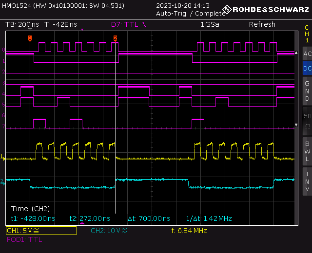
Note that the upper eight purple signals from the logic analyzer are slightly delayed compared to the two analog signals at the bottom, because there are opto couplers in the way. The analog signals are captured from different pins on the board without opto couplers in the way.
The following signals are shown:
| Signal | Description |
| purple 0 | SPI clock (logic analyzer) |
| purple 1 | SPI chip select (logic analyzer) |
| purple 2-7 | 6 least significant bits of SPI MOSI (logic analyzer) |
| yellow 1 | SPI clock (analog channel) |
| blue 2 | SPI chip select (analog channel) |
The cursors measure the length of the analog SPI chip select signal at the bottom, which is exactly 700 ns. This corresponds to the seven clock cycles at 10 MHz, and this is the expected result according to the LUT entries.
This is the corresponding screenshot for running the otherwise identical program with 100 MHz:
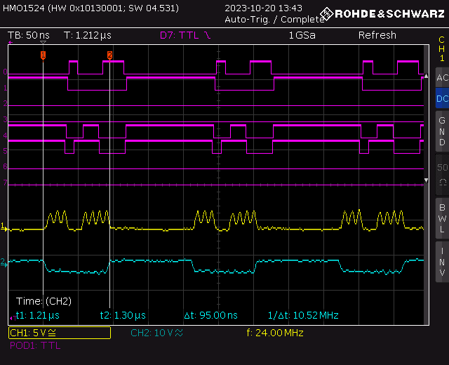
The purple signals of the logic analyzer obviously are no longer reliable, apparently the opto couplers on the board can't keep up anymore.
But with the analog two signals at the bottom we see the following:
- The measurement of the SPI chip select low phase at the bottom reads 95 seconds (blue signal 2). If it was seven cycles at 100 MHz, it should take approx. 70 ns.
- The SPI clock pauses apparently for two cycles after the first three cycles (yellow signal 1).
This is the core of the problem: The FlexSPI engine inserts two dummy cycles on its own, although no dummy cycles are specified in the FlexSPI LUT sequence for the write transaction. The transaction takes nine cycles although it should take only seven cycles. This does happen with an SPI clock frequency of 100 MHz but not with an SPI clock frequency of 10 MHz.
There's nothing we can do about this in software, except from how the FlexSPI engine is configured. This is the configuration of the FlexSPI engine that we use:
    flexspi_config_t config;
    FLEXSPI_GetDefaultConfig(&config);

    config.enableSckFreeRunning = false;
    config.ahbConfig.enableAHBPrefetch    = false;
    config.ahbConfig.enableAHBBufferable  = false;
    config.ahbConfig.enableReadAddressOpt = false;
    config.ahbConfig.enableAHBCachable    = false;
    config.rxSampleClock = kFLEXSPI_ReadSampleClkExternalInputFromDqsPad;
    config.enableCombination = true;

    FLEXSPI_Init(FLEXSPI, &config);

    flexspi_device_config_t deviceconfig = {
        .flexspiRootClk       = 100000000,
        .isSck2Enabled        = 1,
        .flashSize            = 20,
        .CSIntervalUnit       = kFLEXSPI_CsIntervalUnit1SckCycle,
        .CSInterval           = 2,
        .CSHoldTime           = 0,
        .CSSetupTime          = 0,
        .dataValidTime        = 0,
        .columnspace          = 0,
        .enableWordAddress    = 0,
        .AWRSeqIndex          = NOR_CMD_LUT_SEQ_IDX_WRITE,
        .AWRSeqNumber         = 1,
        .ARDSeqIndex          = NOR_CMD_LUT_SEQ_IDX_READ,
        .ARDSeqNumber         = 1,
        .AHBWriteWaitUnit     = kFLEXSPI_AhbWriteWaitUnit2AhbCycle,
        .AHBWriteWaitInterval = 0,
        .enableWriteMask      = false
    };

    FLEXSPI_SetFlashConfig(FLEXSPI, &deviceconfig, FLASH_PORT);
Is there anything wrong with this configuration that could cause the FlexSPI engine to insert dummy cycles that are not specified in the LUT sequence for the FlexSPI write transaction?
Thanks
Stephan
- Mark as New
- Bookmark
- Subscribe
- Mute
- Subscribe to RSS Feed
- Permalink
- Report Inappropriate Content
Hello @stmatscaps,
I hope you are doing well.
Please accept my apology for the delayed response.
Regarding your query I suggest referring to the below link, It will be helpful to comprehend the sequence in detail.
https://elixir.bootlin.com/zephyr/v2.0.0-rc1/source/ext/hal/nxp/mcux/drivers/imx/fsl_flexspi.c
I hope it helps!
Thanks & Regards,
Sanket Parekh
- Mark as New
- Bookmark
- Subscribe
- Mute
- Subscribe to RSS Feed
- Permalink
- Report Inappropriate Content
Hello @Sanket_Parekh ,
I looked at the link that you provided. Could you please be more specific what the relation to my problem is? This link points to the source of an old FlexSPI driver of Zephyr.
We are not using Zephyr but the MCUXpresso SDK. We already studied the fsl_flexspi.c driver source of the MCUXpresso SDK in detail, and at that time we discovered the problem in the implementation of the FLEXSPI_TransferBlocking() function for FlexSPI IP transfers (see preceding post).
But the problem now is with FlexSPI AHB transactions that are triggered by reads and writes to the AHB address space.
Best regards
Stephan
- Mark as New
- Bookmark
- Subscribe
- Mute
- Subscribe to RSS Feed
- Permalink
- Report Inappropriate Content
Hello @Sanket_Parekh ,
we have a workaround, so the issue is resolved, but only after it cost us a lot of time. I think this issue should at least be documented for the FlexSPI driver in the SDK. Ideally the FlexSPI driver should be improved so that it avoids these undesired extra cycles in a write transaction. Do you have a process for requesting this, or should this be reported as an issue in the MCUXpresso SDK GitHub repository?
Thanks
Stephan
- Mark as New
- Bookmark
- Subscribe
- Mute
- Subscribe to RSS Feed
- Permalink
- Report Inappropriate Content
Further testing shows that even after the modification that the FlexSPI transfer is started after filling the IP TX FIFO it still happens that the FLexSPI engine inserts additional dummy cycles after the address part of the transaction although no dummy cycles are specified in the write transaction's LUT entry. We see that with an SPI clock frequency of 100 MHz.
So the question still remains: How can it be avoided that the FlexSPI engine inserts dummy cycles on its own?
- Mark as New
- Bookmark
- Subscribe
- Mute
- Subscribe to RSS Feed
- Permalink
- Report Inappropriate Content
Hello @stmatscaps,
I hope you are doing well.
Please accept my apology for the delayed response.
"What could be causing this unreliable behavior of the FlexSPI peripheral? "
->LUT is programmed by software with command sequences which is used to issue memory commands.
Please make sure to check section 6.1.5.2.1 FlexSPI Configuration Block
lutCustomSeqEnable -> set the offset accordingly whether if Use pre-defined LUT sequence index and number then set it as 0 or else 1
Please also refer to the Section 10.2.2 Glossary for the FlexSPI module for more details.
Along with that Section 10.2.4.7 Look Up Table will be helpful.
Please refer to these suggestions.
Thanks & Regards,
Sanket Parekh
