- Forums
- Product Forums
- General Purpose MicrocontrollersGeneral Purpose Microcontrollers
- i.MX Forumsi.MX Forums
- QorIQ Processing PlatformsQorIQ Processing Platforms
- Identification and SecurityIdentification and Security
- Power ManagementPower Management
- Wireless ConnectivityWireless Connectivity
- RFID / NFCRFID / NFC
- Advanced AnalogAdvanced Analog
- MCX Microcontrollers
- S32G
- S32K
- S32V
- MPC5xxx
- Other NXP Products
- S12 / MagniV Microcontrollers
- Powertrain and Electrification Analog Drivers
- Sensors
- Vybrid Processors
- Digital Signal Controllers
- 8-bit Microcontrollers
- ColdFire/68K Microcontrollers and Processors
- PowerQUICC Processors
- OSBDM and TBDML
- S32M
- S32Z/E
-
- Solution Forums
- Software Forums
- MCUXpresso Software and ToolsMCUXpresso Software and Tools
- CodeWarriorCodeWarrior
- MQX Software SolutionsMQX Software Solutions
- Model-Based Design Toolbox (MBDT)Model-Based Design Toolbox (MBDT)
- FreeMASTER
- eIQ Machine Learning Software
- Embedded Software and Tools Clinic
- S32 SDK
- S32 Design Studio
- GUI Guider
- Zephyr Project
- Voice Technology
- Application Software Packs
- Secure Provisioning SDK (SPSDK)
- Processor Expert Software
- Generative AI & LLMs
-
- Topics
- Mobile Robotics - Drones and RoversMobile Robotics - Drones and Rovers
- NXP Training ContentNXP Training Content
- University ProgramsUniversity Programs
- Rapid IoT
- NXP Designs
- SafeAssure-Community
- OSS Security & Maintenance
- Using Our Community
-
- Cloud Lab Forums
-
- Knowledge Bases
- ARM Microcontrollers
- i.MX Processors
- Identification and Security
- Model-Based Design Toolbox (MBDT)
- QorIQ Processing Platforms
- S32 Automotive Processing Platform
- Wireless Connectivity
- CodeWarrior
- MCUXpresso Suite of Software and Tools
- MQX Software Solutions
- RFID / NFC
- Advanced Analog
-
- NXP Tech Blogs
- Home
- :
- Model-Based Design Toolbox (MBDT)
- :
- NXP Model-Based Design Tools Knowledge Base
- :
- Example Model: RDDRONE-BMS772
Example Model: RDDRONE-BMS772
- Subscribe to RSS Feed
- Mark as New
- Mark as Read
- Bookmark
- Subscribe
- Printer Friendly Page
- Report Inappropriate Content
Example Model: RDDRONE-BMS772
Example Model: RDDRONE-BMS772
Introduction
The RDDRONE-BMS772 is a standalone BMS reference design suitable for mobile robotics such as drones and rovers, supporting 3 to 6 cell batteries.
The main components mounted on the board are:
- MCU: S32K144 (S32K1 Microcontroller for General-Purpose);
- BCC: MC33772B (6 Channel Li-Ion Battery Cell Controller IC);
- SBC: UJA1169TK (Mini High-Speed CAN System Basis Chip);
- RFID: NTAG5-Boost (NTAG 5 Boost: NFC Forum Compliant I2C Bridge for Tiny Devices)
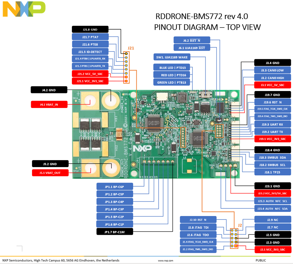
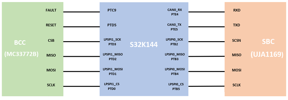
An overview of the pins available on the board and the connections between ICs can be consulted below. For further details, please check the datasheet and schematic available on the product's page.
Prerequisite software
To create, build and deploy a Simulink model onto the RDDrone BMS772, the following software is required:
- MATLAB® R2016a or later
- S32K1xx MBDT Toolbox Version 4.3.0
- JLink Debug Probe Segger
- FreeMASTER Run-Time Debugging Tool
Prerequisite hardware
The hardware required for this example is:
- RDDrone BMS772
- CAN Bus Terminator resistor (DRONE-CAN-TERM)
- OLED Display 128x32 pixels
- 12V DC Power Supply (it's not included in the RDDRONE kit)
- External Thermistor with cable
- CAN interface for USB
- 6-Cell Battery Emulator (it requires a separate 12V DC power supply, consult User Manual)
- JLink Debug Probe
- Soldering iron: By default, the BCC is configured to work with a 3S configuration. To configure for 4S, 5S or 6S, multiple modification must be performed on the board. (Consult SPF-45742 for further details)
Create the model and configure the components
Initialize the model
To configure a model to work with blocks from S32K1xx toolbox, the MBD_S32K1xx_Config_Information block must be added.
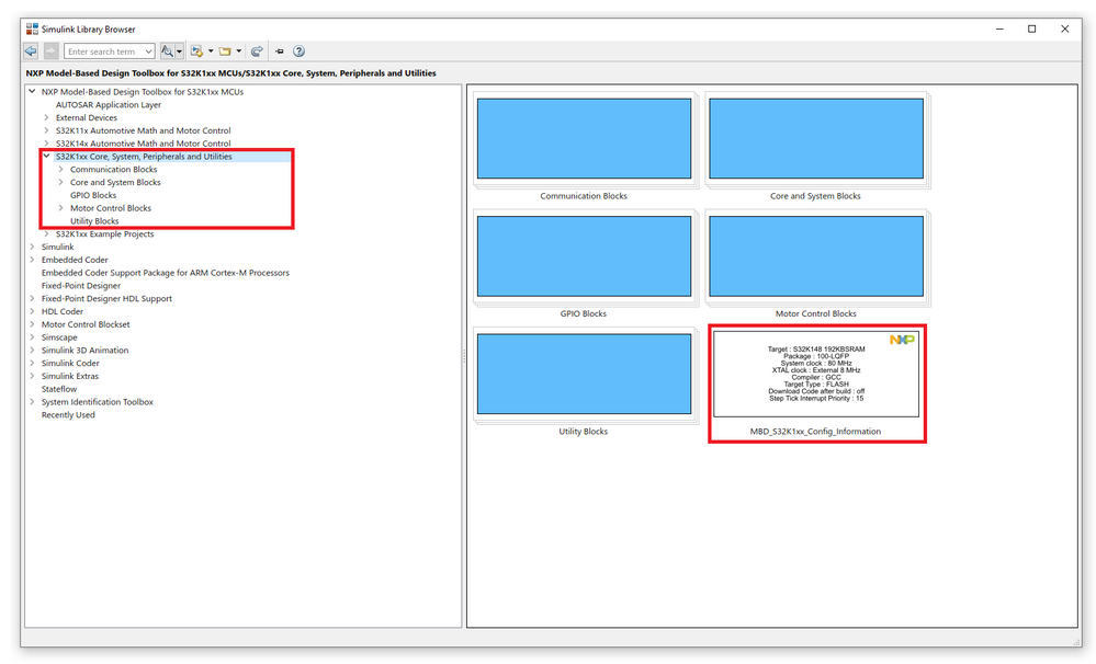
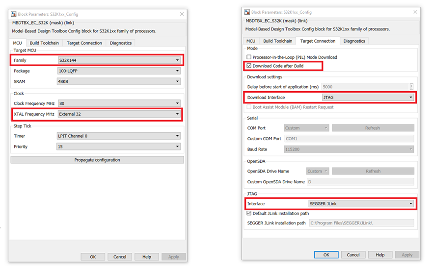
The RDDRONE is part of S32K144 family, with an External 32 MHz external crystal. The download interface is JTAG, using the Segger Link.
Note! Segger JLink Software is not included in the toolbox and must be installed separately.
Initialize System Basis Chip
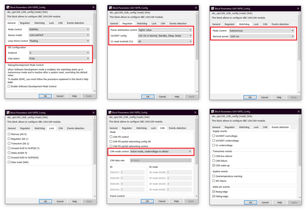
The System Basis Chip (SBC) mounted on the board is UJA1169TK, which is a mini high speed CAN transceiver. Moreover, it also features a watchdog and it can be configured via LPSPI0 (Low Power Serial Peripheral Interface).
Out of the box, the SBC is running in Forced Normal Mode, which means that the watchdog is disabled, but CAN transceiver continues to work. If the SBC is initialized and configured, it exits the Forced Normal mode and enters Normal Mode operation. Now, the watchdog must be reset accordingly to the configuration made, otherwise it will trigger a reset.
A special operation mode is Software Development Mode Control and it allows the SBC to be configured (CAN, power regulator) while the watchdog is kept disabled. To enable the SDMC, the SBC must be in Forced Normal Mode (Further details can be found here: 7.11.2 Restoring factory preset values).
Note! MCU configures the SBC via the SPI. Therefore, the LPSPI0 must be initialized before the SBC config block.

A basic configuration for SBC can be found below.
Initialize FreeMASTER
FreeMASTER is a user-friendly real-time debug monitor and data visualization tool that enables runtime configuration and tuning of embedded software applications. The connection between MCU and FreeMASTER application can be done via the following:
- UART
- CAN
- Debugger Probe/On-board debugger interface
In this example, the CAN0 interface is used to send/receive messages from FreeMASTER application. The RxD and TxD pins required are PTE4, respectively PTE5 (both are routed to J3 connector). The default bitrate is 1000 Kbit/s but depending on the use case, it can be lowered.
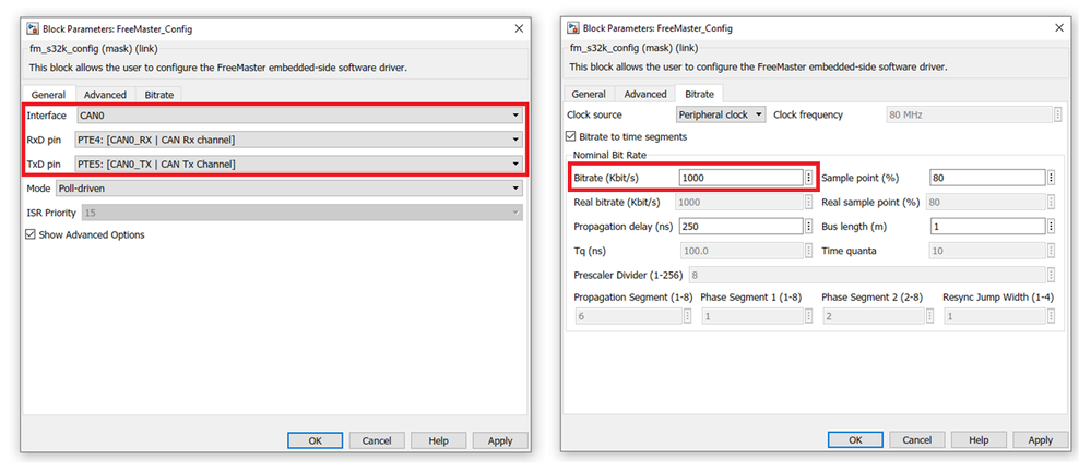
Note! FreeMASTER can add a lot of overhead if the user interface monitors multiples variables at a very fast refresh rate, and it can cause the step function to overrun.
Initialize BCC
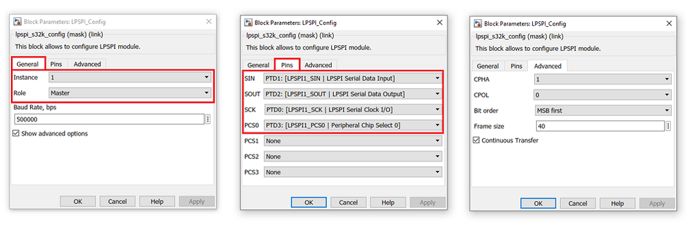
Battery Cell Controller (BCC) MC33772B can be configured and used by the MCU via SPI/TPL. Similar to SBC, the communication interface (LPSPI1) must be initialized before initializing the BCC. As a feature, the BCC block can assist you to configure the LPSPI interface to properly work.
First of all, add the LPSPI config block and select the instance to 1 (as this instance is routed on the RDDRONE board from the MCU to the MC33772B). Go to Pins tab and select the pins used by LPSPI1 and BCC. The role, baud rate and other advanced settings are going to configured later from the BCC config block.
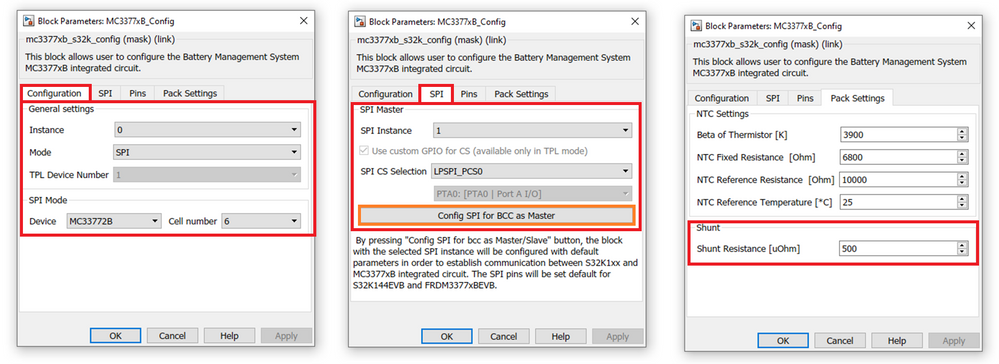
As there are no TPL transceiver added, the MC33772B communicates with the MCU via LPSPI instance 1 (previously configured). In the General tab, Instance refers to the instance of the BCC (not to be confused with the LPSPI instance). In the area "SPI Mode", the type of the BCC must be selected. In this case, the BCC mounted on the RDDRONE is MC33772B. The number of cells is 6.
Going next to the SPI tab, the SPI Instance needs to be set to 1 and the SPI CS Selection to LPSPI_PCS0.
Lastly, in the Pack Settings, it is a must to set Shunt Resistance to 500 uOhm (as this is the value of the shunt resistor R1 mounted on the board).
- Configuration Tab
- General Settings
- Instance: 0
- Mode: SPI
- SPI Mode
- Device: MC33772B
- Cell number: 6
- General Settings
- SPI tab
- SPI instance: 1
- SPI CS Selection: LPSPI_PCS0
- Pack Settings
- Shunt resistance: 500 uOhm (shunt resistor R1 is mounted directly on the RDDRONE)
Note! MCU configures the BCC via the SPI. Therefore, the LPSPI1 must be initialized before the MC33772B config block.
Initialize SSD1306 OLED
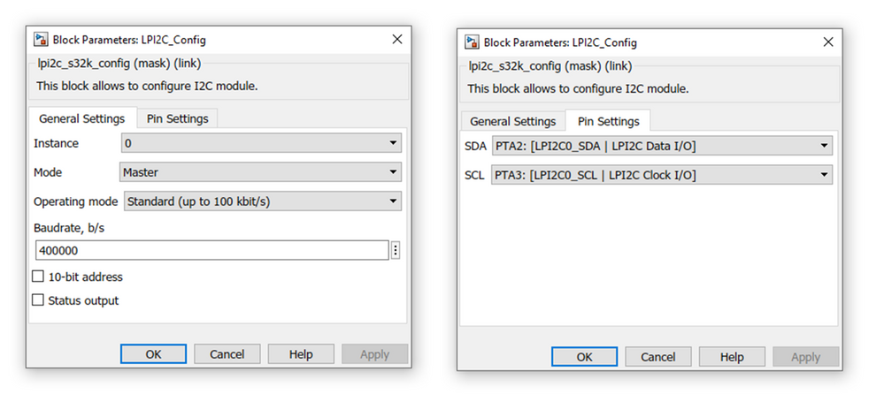
The OLED display used in this example is a 128 x 32 pixels display that communicates with the MCU via LPI2C0 (J23).
The configuration for LPI2C is presented below:
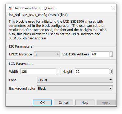
After the LPI2C is configured, the block to configure the OLED can be added and configured as below:
- LPI2C Instance: 0
- SSD1306 Address: 60 (represented in decimal format, hex: 0x3C)
- Width: 128
- Height: 32
- Font: 11 x 18
- Background color: Black
Note! MCU configures the LCD via the I2C. Therefore, the LPI2C0 must be initialized before the LCD config block.
Initialize Gate Driver
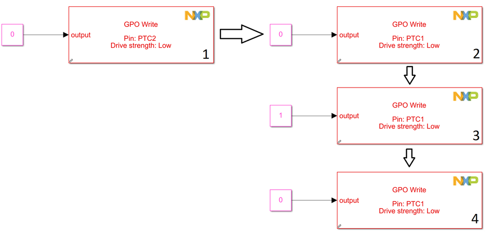
The gate driver is controlled by a D-type flip flop and it allows the MCU to disconnect the electrical load (motors, servos) attached to Power OUT pads from the Power IN, when the battery is discharged or various faults occurs.
GPIO PTC2 is connected to the 'Data input' pin of the D-type flip flop (U10) and it is active low (set pin to 0 to enable the gate driver and to 1 to disable it). GPIO PTC1 is connected to the 'CLK' pin of the flip flop which is a rising edge triggered clock signal input pin. So, to control the gate driver, the PTC2 must be set to the desired state, then the PTC1 is toggled 2 times. To assure that the sequence is kept in order, set the priority of each GPIO Write block.
Structure of the application
One of the most recommended design style for an application in Simulink with NXP MBD Toolbox is to break down the application into three categories as:
- Input: Hardware dependent blocks that read/receive the values of interest from peripherals
- Algorithm: Hardware independent blocks that process the values received from the Input blocks.
- Output: Hardware dependent blocks which receive the processed values from the Algorithm blocks
One advantage of this approach is that a fully tested application can be converted to new hardware without any modification to the ALGORITHM part. Only the INPUT and OUTPUT blocks must be updated to the new hardware. Moreover, while developing an application, you can validate the ALGORITHM section in Software-in-the-Loop (SIL) or Processor-in-the-Loop (PIL). These two methods of simulation are useful to test cases that are not easy to replicate, as specific data can be fed as input.
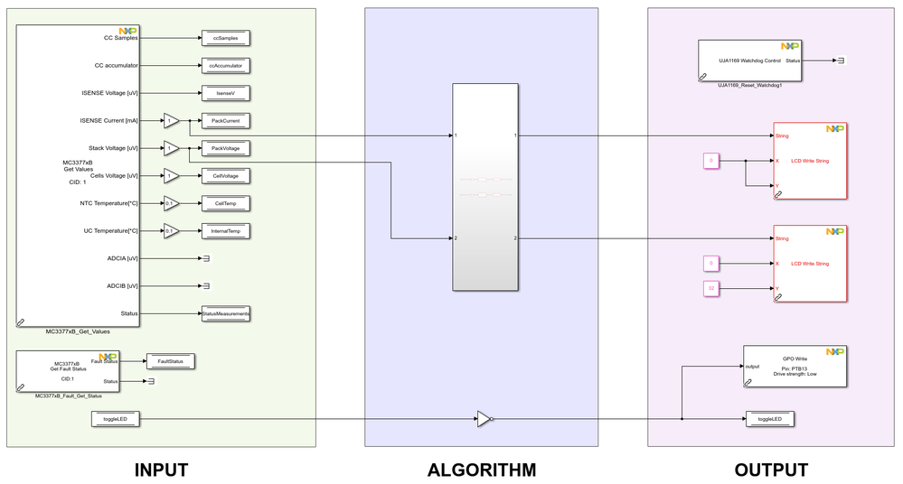
Taking these into account, this example can be structured like this:
- Input (green area):
- The blocks in this area read data from the MC3377xB BCC and store them in multiple data stores.
- In case there are any faults detected, MC3377xB_Fault_Get_Status reads the error and store it in FaultStatus data store memory.
- To make sure the MCU is not halted, an onboard LED (PTB13) is toggled at each step.
- Algorithm (blue area):
- As this example is more of a dummy one, the algorithm part only processes the PackVoltage and PackCurrent to be properly displayed on the OLED display.
- toggleLED variable is negated at every step to toggle the onboard LED.
- OUTPUT (pink area)
- Reset the SBC UJA116x's watchdog to avoid the forced restart of the board
- PackVoltage and PackCurrent received in INPUT area and processed in ALGORITHM area is then shown on the OLED display.
- Toggle the LED and save the new value in toggleLED data store memory.
Deployment
Now that the application is completed (make sure the steps at Create the model and configure the components -> Initialize the model are correctly followed), it can be deployed on the target.
First of all, the JLink probe must be correctly connected to the RDDRONE board to the J2 header. Then, power the board using a 12V power supply by using the J4 pads.
Important! When soldering the header on J4 pads, make sure the polarity is properly respect, otherwise, you might risk to permanently damage the board.
The CAN analyzer must be connected to J3 and the CAN terminator to J20 (located on the back of the board, right below J3 header).
OLED display must be inserted into J23 header.
Important! Make sure to properly respect the polarity of the display, otherwise you might risk to permanently damage the display.
The 6 Cell Battery Emulator must be connected to the JP1 header. Depending on the configuration made on the back of the RDDrone, connect the cells to its respective pin on the board (consult the overview pinout presented at the beginning of the article). Pin JP1[7] must be connected to the CTREF[33] pin of the battery emulator.
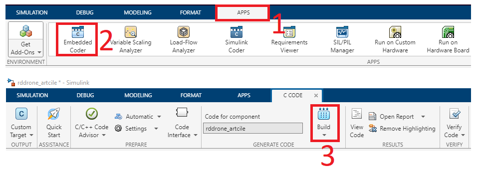
Finally, the code can be generated based on the Simulink model, compiled and deployed on the target. To do this, go to Simulink -> Apps -> Embedder Coder then click on the Build button.
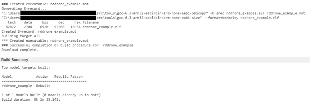
Now, in the Diagnostic Viewer, the deployment process can be analyzed to see if there are any errors with the application and if the download was successfully completed on the target like in the image below, where we can see:
- The .elf file is successfully generated and its size
- The download is completed
Important! In order to be able to download code on the target, the reset line from the SBC to S32K144 must be disconnected, remove the header on J5 during the deployment process.
FreeMASTER
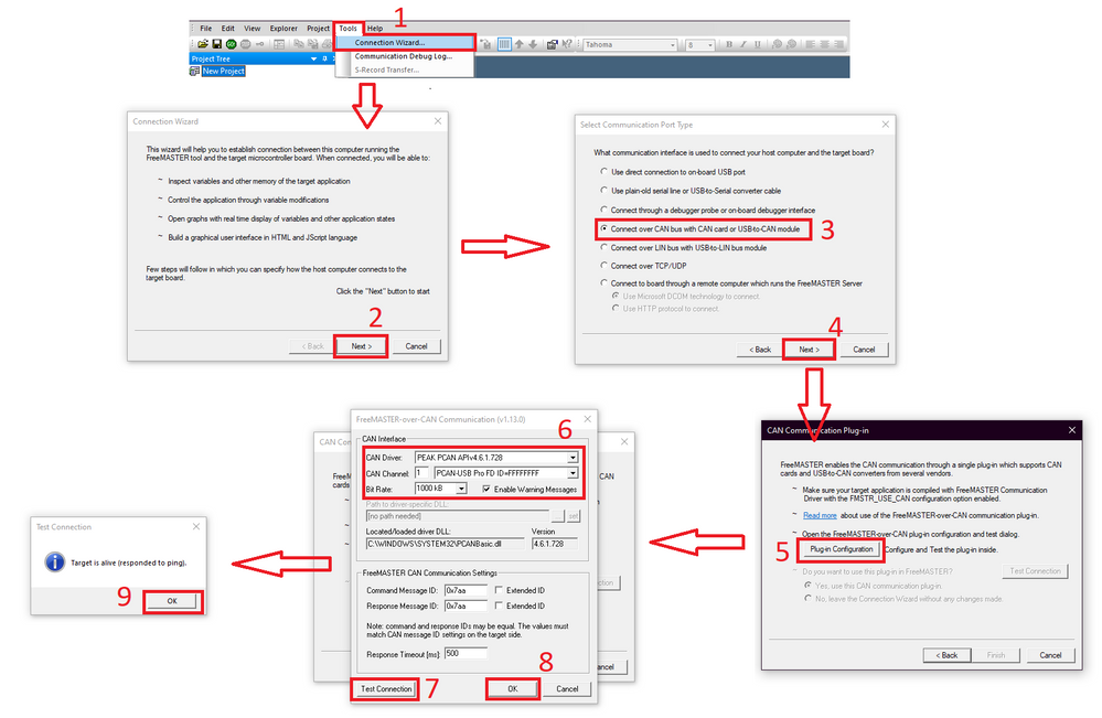
Now that the application is deployed on the target, FreeMASTER can be configured to connect to the target via CAN. Go to the TOOLS -> Connection Wizard and select the Connect over CAN BUS with CAN card or USB-to-CAN module. In the prompted window, configure the CAN Interface accordingly to your hardware and configuration made in the Simulink model.
Now that the FreeMASTER connection with target is completed, the .ELF file must be selected to access variables and monitor them in real-time.
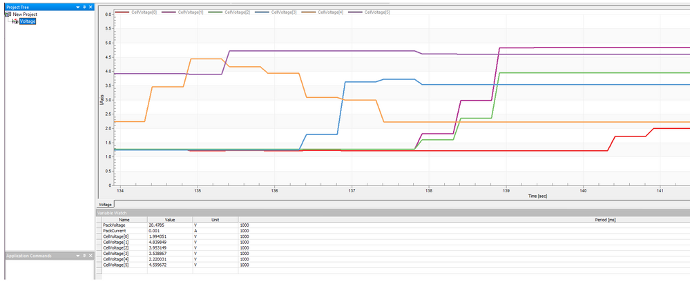
Finally, start the communication between FreeMASTER and the target and the data shown should be similar to this:
Conclusion
In this article, we described how to use NXP Model Based Design Toolbox for S32K1xx to handle a custom hardware design (such as RDDRONE BMS772), from the configuration of the peripherals to the download on the target and validating the application. The example covers all the peripherals that the S32K1xx toolbox 4.3.0 supports for the RDDRONE. Feel free to comment below if you have questions.
NXP is a trademark of NXP B.V. All other product or service names are the property of their respective owners. © 2023 NXP B.V. Arm, Cortex are trademarks and/or registered trademarks of Arm Limited (or its subsidiaries or affiliates) in the US and/or elsewhere. The related technology may be protected by any or all of patents, copyrights, designs and trade secrets. All rights reserved. MATLAB, Simulink, Stateflow and Embedded Coder are registered trademarks and MATLAB Coder, Simulink Coder are trademarks of The MathWorks, Inc. See mathworks.com/trademarks for a list of additional trademarks.
- Mark as Read
- Mark as New
- Bookmark
- Permalink
- Report Inappropriate Content
Free master over serial is working but not over CAN as in the given example. downloading the pre-compiled binary works so the issue is not the physical CAN wiring but the Simulink build process seems broken for 2023b.
The build process does not generate any errors, and the only significant warning present in the Diagnostics section of the model is that the priority order for the "Initialize Gate Driver" subsystem has been ignored.
