- Forums
- Product Forums
- General Purpose MicrocontrollersGeneral Purpose Microcontrollers
- i.MX Forumsi.MX Forums
- QorIQ Processing PlatformsQorIQ Processing Platforms
- Identification and SecurityIdentification and Security
- Power ManagementPower Management
- Wireless ConnectivityWireless Connectivity
- RFID / NFCRFID / NFC
- Advanced AnalogAdvanced Analog
- MCX Microcontrollers
- S32G
- S32K
- S32V
- MPC5xxx
- Other NXP Products
- S12 / MagniV Microcontrollers
- Powertrain and Electrification Analog Drivers
- Sensors
- Vybrid Processors
- Digital Signal Controllers
- 8-bit Microcontrollers
- ColdFire/68K Microcontrollers and Processors
- PowerQUICC Processors
- OSBDM and TBDML
- S32M
- S32Z/E
-
- Solution Forums
- Software Forums
- MCUXpresso Software and ToolsMCUXpresso Software and Tools
- CodeWarriorCodeWarrior
- MQX Software SolutionsMQX Software Solutions
- Model-Based Design Toolbox (MBDT)Model-Based Design Toolbox (MBDT)
- FreeMASTER
- eIQ Machine Learning Software
- Embedded Software and Tools Clinic
- S32 SDK
- S32 Design Studio
- GUI Guider
- Zephyr Project
- Voice Technology
- Application Software Packs
- Secure Provisioning SDK (SPSDK)
- Processor Expert Software
- Generative AI & LLMs
-
- Topics
- Mobile Robotics - Drones and RoversMobile Robotics - Drones and Rovers
- NXP Training ContentNXP Training Content
- University ProgramsUniversity Programs
- Rapid IoT
- NXP Designs
- SafeAssure-Community
- OSS Security & Maintenance
- Using Our Community
-
- Cloud Lab Forums
-
- Knowledge Bases
- ARM Microcontrollers
- i.MX Processors
- Identification and Security
- Model-Based Design Toolbox (MBDT)
- QorIQ Processing Platforms
- S32 Automotive Processing Platform
- Wireless Connectivity
- CodeWarrior
- MCUXpresso Suite of Software and Tools
- MQX Software Solutions
- RFID / NFC
- Advanced Analog
-
- NXP Tech Blogs
- Home
- :
- トピック
- :
- NXP Designs ナレッジベース
- :
- Design your NFC Antenna with NXP’s OM29263ADK development kit
Design your NFC Antenna with NXP’s OM29263ADK development kit
- RSS フィードを購読する
- 新着としてマーク
- 既読としてマーク
- ブックマーク
- 購読
- 印刷用ページ
- 不適切なコンテンツを報告
Design your NFC Antenna with NXP’s OM29263ADK development kit
Design your NFC Antenna with NXP’s OM29263ADK development kit
This post entry provides a detailed description of the OM29263ADK kit, a new antenna tuning development kit specially designed to facilitate the NFC antenna prototyping process. This document has been structured as follows:
- OM29263ADK kit contents
- Using OM29263ADK kit with CLEV6630A or CLEV6630B
- Using OM29263ADK kit with PNEV5180B or PNEV7462C
- Using OM29263ADK kit to connect your own antenna coil
- Define target impedance and Q-factor
- Measure antenna coil
- Design EMC filter
- Calculate matching circuit components
- Assemble and measure
- Adjust receiver circuit
- Using OM29263ADK kit to evaluate the performance of different antenna shapes
- Background information
- Coupling coefficient
- Mutual inductance
- Antenna tuning components used for the large antenna
- Antenna tuning components used for the small antenna
- OM29263ADK large antenna vs small antenna
- ISO/IEC14443 vs ISO/IEC15693 reader - Quality factor
- Further information
- Video recorded session
OM29263ADK kit contents
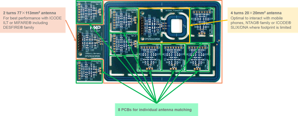
This kit consists of a single PCB board that includes:
- A pre-matched antenna of 2 turns and a size of 77 by 113 mm.
- A second pre-matched antenna of 4 turns and a smaller size of 20 by 20 mm.
- And, 8 extra boards to prepare the matching for custom antennas.
As a result, this kit is a perfect resource for different purposes such as evaluating the RF performance of different antenna sizes and, for prototyping your custom antenna quickly. In addition, this NFC antenna development kit is compatible with our existing product support package. You can directly connect it to CLRC663 demoboards, as well as to PN5180 and PN7462 demoboards after a minor tuning.
Using OM29263ADK kit with CLEV6630A or CLEV6630B
The process is really straightforward…
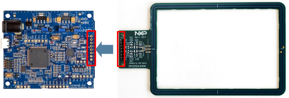
- First, take one CLRC663 demoboard and separate the main PCB from the antenna & matching circuit. The board includes cut lines, so you can divide both sections easily by only using your hands.
- Second, break the kit OM29263ADK PCB so that you separate the pre-matched antenna from the other PCB parts.
Then, it is just a matter of connecting the two parts together.
- The kit antenna includes pin male connectors while the CLRC663 board includes the corresponding female connectors.
- Therefore, hook up the antenna with the main board, solder the connectors and that’s all.
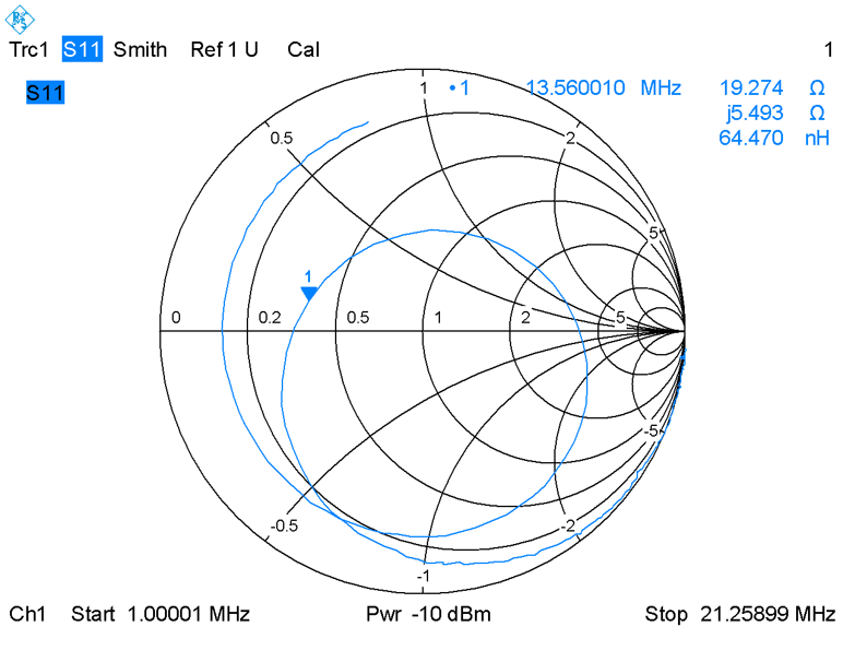
We can observe that when we connect the kit large antenna to the reader PCB, the impedance measured with our network analyzer shows that the tuning is adjusted to approximately, 19 Ohms. This is the result obtained without any hardware modification
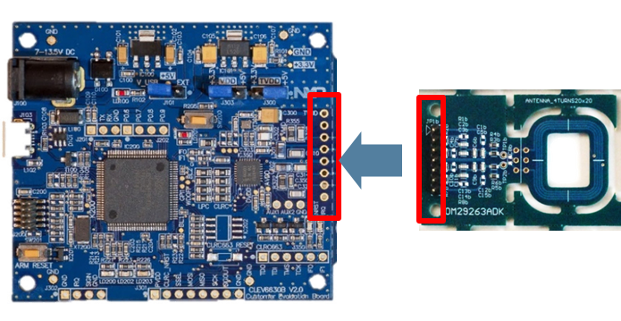
The same process applies for the smaller antenna:
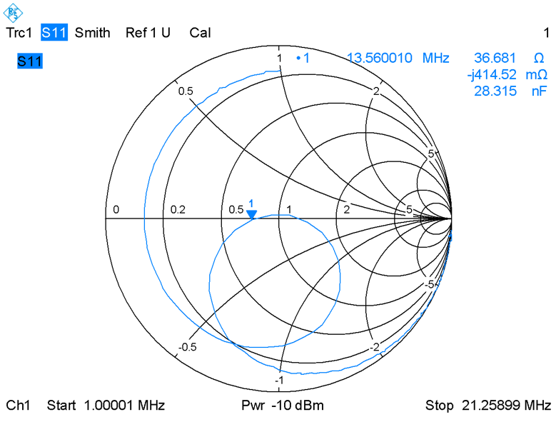
Similarly, we can observe that when we connect the kit small antenna to the reader PCB, the impedance measured with our network analyzer shows that the tuning is adjusted to approximately, 36 Ohms. This is the result obtained without any hardware modification:
Using OM29263ADK kit with PNEV5180B or PNEV7462C
In case you are interested to connect the OM29263ADK kit antennas to the PNEV5180B or PNEV7462C boards, the preparation process is the following:
- First, separate the antenna and the matching section from the PN5180 or PN7462 demoboards, as before, using the cut lines.
- Then, take one kit sample, and separate the pre-matched antennas for the other PCB parts.
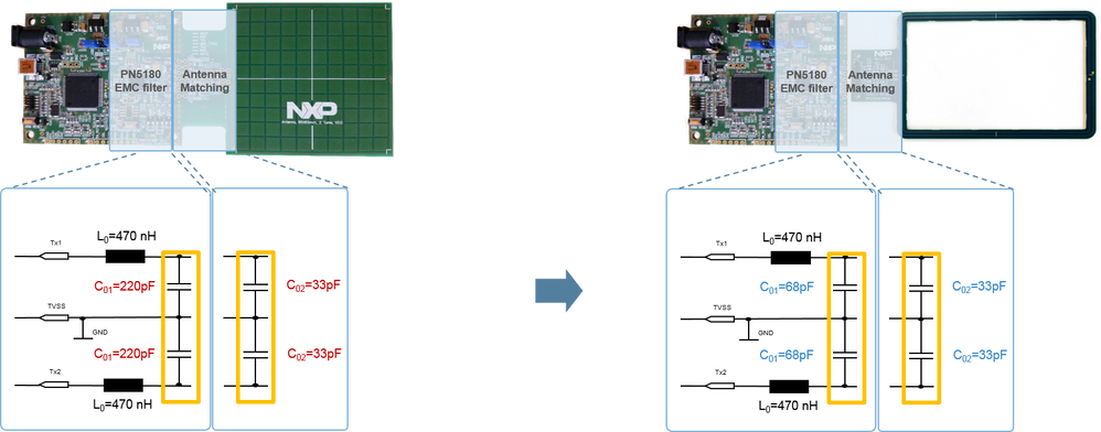
- And finally, adjust the EMC filter.
The EMC filter adaptation is required because the kit antenna is prepared for asymmetric tuning while the PN5180 and PN7462 original antenna use a symmetrical tuning. The main difference between both types of tuning is the cut off frequency. The symmetric tuning uses a cutoff frequency around 15MHz, while the asymmetric can go up to 22 MHz. In practice, for this adaptation, we only need to change the value of the capacitor C0 in the main board. For instance, the existing 220 pF capacitor can be replaced for another one of 68 pF.
Using OM29263ADK kit to connect your own antenna coil
This section describes how to use the kit PCB boards for our custom antenna tuning. For this task, the list of material that we need is:
- A reader PCB board, in the example, we picked CLRC663
- One of the PCBs for antenna matching included in the kit
- And, the any antenna to be matched In our case, we have selected one sample antenna available in our lab.
The following explanation will be guided using this antenna as a reference, but any antenna can be tune using the same process.
The usual list of steps to tune a custom antenna are:
- First, we need to define target impedance and Q factor, as design parameters for our reader
- Then, we will characterize the antenna coil and find its parameters
- After that, we will design the EMC filter
- With this, we will calculate the matching components using an Excel sheet
- Afterwards, we will assemble the calculated components and measure the first results.
- We will take field measurements, which probably will show that it is not perfect, so we may need to adapt the matching values
- With these fine-tuned vales, we will re-assemble again
- And finally, we will design the receiver circuit.
Define target impedance and Q-factor
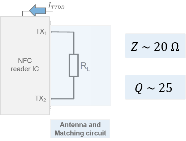
First, we start defining the target impedance and Q-factor. The target impedance is a design parameter, which needs to be chosen according to our needs whether we want to go for maximum field strength or minimum battery consumption or a trade-off in between. Typically, reasonable values are between 20 Ohms and 80. Another important design parameter is the Q factor. The Q factor is a dimensionless parameter indicating the performance of a resonant circuit. The higher the Q factor, the higher the read range. On the other hand, increasing the Q factor also reduces the bandwidth of the circuit. As a result, in practical implementation, Q-factor values below 30 are demonstrated to fit well for the ISO14443 wave form timing requirements and corresponding spectrum. For our tuning exercise, the design parameters chosen are an impedance of 20 ohms and a Q factor of 25
Measure antenna coil
Next step is to characterize the antenna coil. Any antenna coil has an input impedance. This input impedance is complex and consists of an inductance, capacitance as well as some losses represented by a resistance (R). The actual values depend, among others, on antenna material, thickness of conductor, distance between the windings, number of turns, etc.
The coil characterization needs to be done with a network analyzer. It could be a high end, such as Agilent or Rohde & Schwarz, which is powerful, accurate, easy to use, but expensive. Or we can also go for low end solutions, such as the miniVNA PRO, which is cheap compared with the previous ones, and accurate enough for our needs. In our case, the characterization of our lab antenna shows:
- An inductance around 1.3 uH
- And a resistance of 2.5 Ohms
Design EMC filter
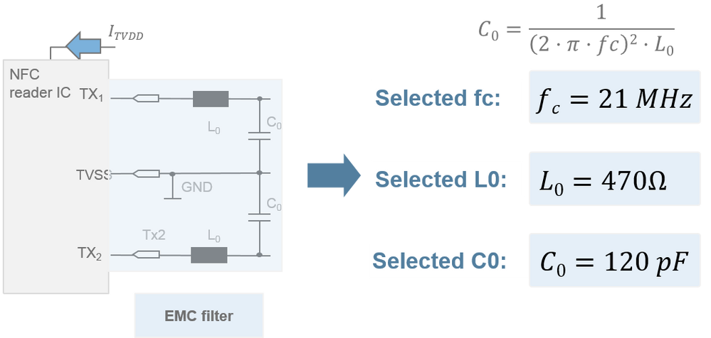
The next step is to design the EMC filter. As we are using CLRC663, we will go for an asymmetric antenna tuning. Good inductor values are between 330nH and 560nH. and 21MHz cutoff frequency is ideal for asymmetric tuning. Fixing this two parameters, we can easily calculate the required capacitor component for our EMC filter with the formula below. In our example, we need to use a capacitor of C= 122 pF. With this, we just pick up the closer commercial value from our components box
Calculate matching circuit components
We have characterized the antenna coil and completed the EMC filter. Now, we can calculate the matching network components. The matching components need to be calculated so that the maximum power from the reader is transmitted to the antenna. This happens when the equivalent impedance seen from the reader IC only has the real part, without the complex part.
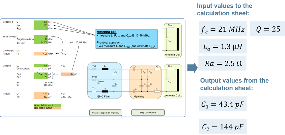
There are some complex calculation involved in the process. In order to avoid these cumbersome formulas, NXP provides a useful Antenna Tuning excel sheet that calculate the appropriate components for you. Below, you can see a screenshot of the Excel sheet in the slide.
This sheet calculates C1 and C2 matching values according to the inputs expected from the user. These are
- The measured antenna coil parameters
- The EMC filter parameters.
- The target impedance and Q-factor of our design
With these values, The Excel sheet calculates and outputs the value of the matching components: C0, C1, C2 and Rs. In our exercise, the output values calculated for the matching network by the Excel sheet are C1 around 43 pF and C2 around 144 pF
Assemble and measure
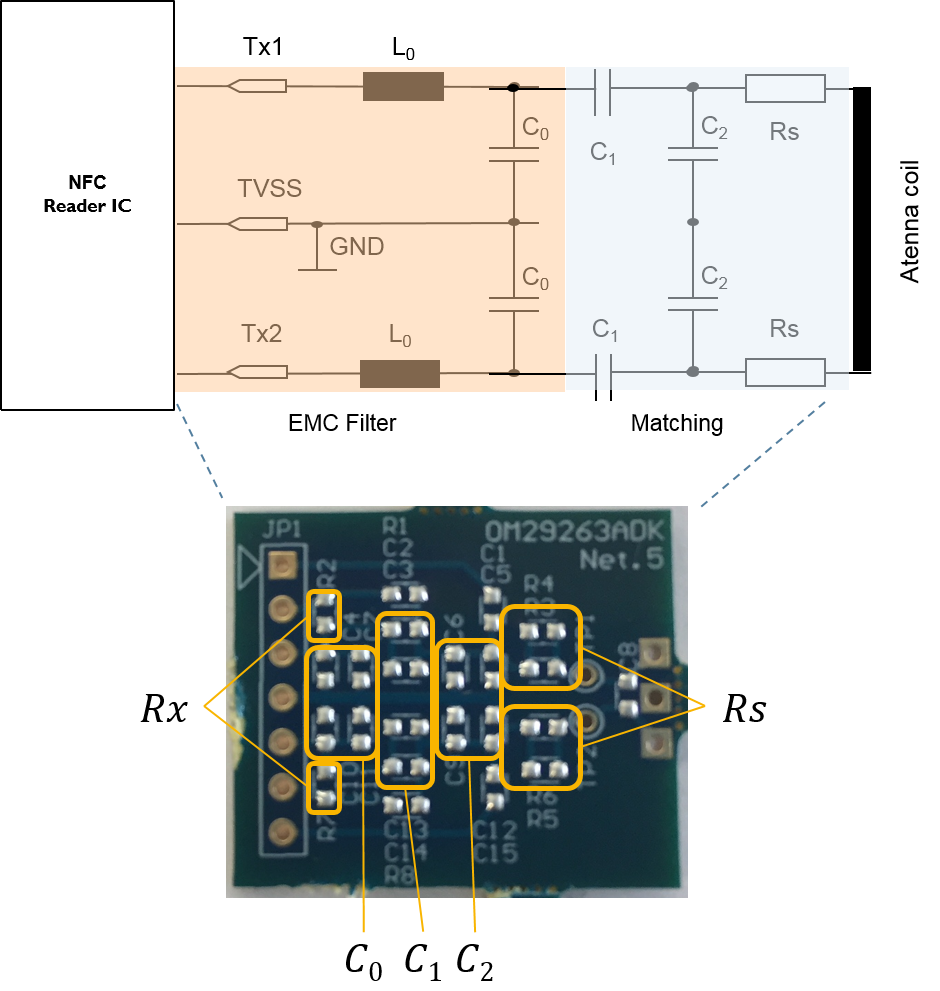
Typically, the calculated values do not match with commercial components. The easiest way is to add components in parallel to get as close as possible to the calculated values. If we take a closer look to the kit antenna matching PCB board, the pad location is the following:
- We have two slots for C0 – so we can have two capacitors in parallel to achieve a better accuracy on the capacitance value we need to achieve
- We also have two slots for C1, for the same purpose
- We have two more slots for C2 soldering
- We also have two slots for the dampening resistor, in case we need to reduce the Q-factor of our antenna.
- And finally, one slot for the receiver resistor circuit.
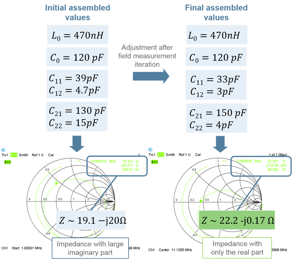
After the first component assembly, it is worth performing a field measurement to find out how accurate our matching is in reality. Typically, the measured impedance is different than the impedance calculated in the simulation. Therefore, the calculated matching components were not 100% accurate. But we knew that in advance. We were aware that we were just getting a rough approximation to the antenna parameters. As a result, a good matching is achieved after a number of iterations according to the field measurements that we obtain. As a general rule, C1 changes the magnitude of the matching impedance and C2 changes its imaginary part.
In our exercise, after soldering the first components, the equivalent impedance is around 19 Ohms but it also has a significant imaginary part. As a result, it can be fine-tuned towards better performance. We modified C1 and C2 a couple of times until we found out the final values that work better. obtaining a impedance with only real part at 22 Ohms (C1= 36pF and C2=154 pF).
Adjust receiver circuit
The last step of tuning our antenna is to design the receiver circuit. The Rx circuit that consists of a voltage divider and a coupling capacitor connected from the output of the EMC filter to the RX pins of the NFC reader. The objective is to set the voltage level at the reception pins to achieve the compromise between a good sensitivity. For CLRC663 plus, the serial resistor is in the range of 7 and 15 kΩ. You can start with a 11 KOhm value, then, the resistor can be adjusted depending on the voltage measured in the Rx pins. If the voltage at Rx pin is higher than 1.7 V, it is recommended to increase the resistor value and if the voltage at Rx pin is below than 1.2 V, it is recommended to decrease the resistor value.
Using OM29263ADK kit to evaluate the performance of different antenna shapes
The section covers how you can use the antennas included in the kit for performance comparison. Please note that this lab exercise is shown only for illustrative purposes on how the kit can be used to evaluate the performance of different antenna shapes.
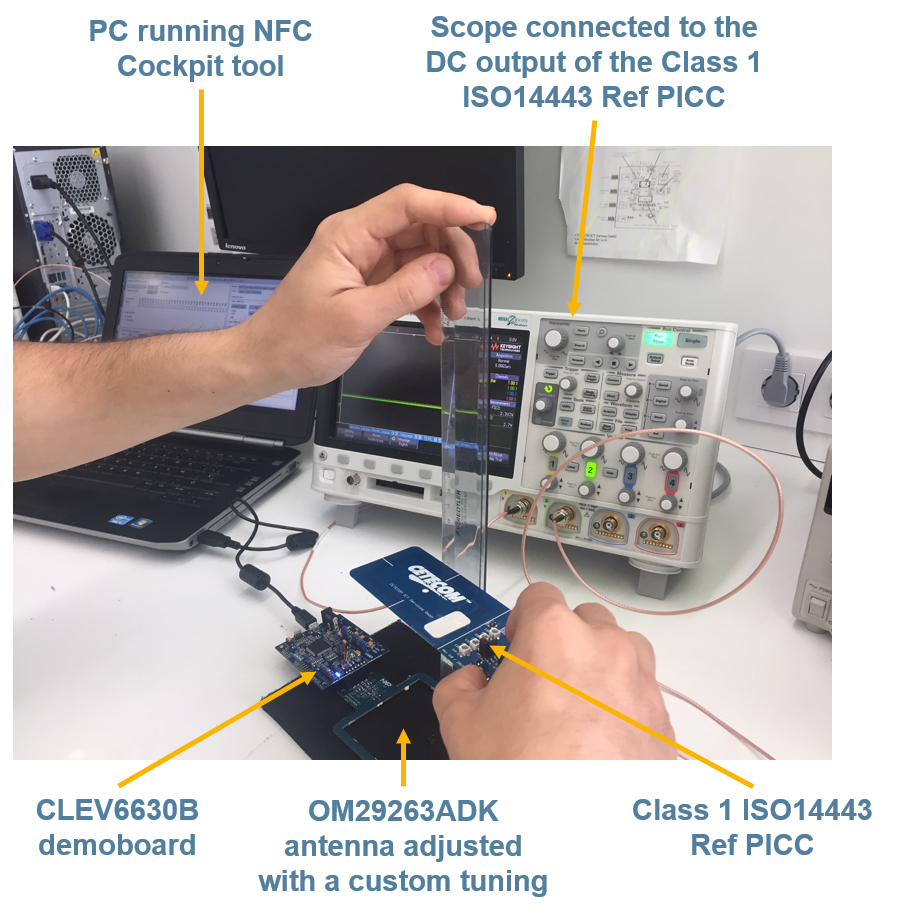
As an example, we defined a sample scenario where we want to characterize how the field strength decreases with distance when using antennas of different size. For that, we used the following setup:
- A class 1 ISO14443 Reference PICC
- A scope
- A CLRC663 board connected to the small antenna
- A CLRC663 board connected to the large antenna
- A ruler to measure the distance
The measurements were taken in this way:
- We tuned the large and small antennas to 20 Ohms
- We connected the board to the laptop, and we executed the NFC Cockpit tool to control the RF field.
- We measured with the scope the voltage level obtained by the ISO14443 Class 1 Reference PICC while we increased the distance.
Background information
Before actually showing you the results, it is worth it to review a couple of antenna design principles to properly understand the results.
Coupling coefficient
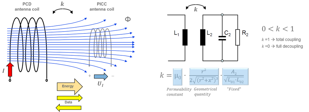
Before actually showing you the results, it is worth it to review a couple of antenna design principles to properly understand the results. The coupling coefficient is a parameter that indicates how much of the magnetic field generated by the reader is picked up by the card. The coupling coefficient takes a value between 0 and 1
- If the coupling equals 1, it means we have a perfect coupling, all magnetic field lines are picked by the card
- If the coupling equals 0, it means we have no coupling at all, no magnetic field lines are picked by the card
The key message is that the coupling coefficient is just a geometric quantity. It depends on:
- The reader and card antenna dimensions (both antenna radius)
- Their relative position (whether in parallel or perpendicular, they will pick a different amount of magnetic field lines)
- The distance between them
- And the magnetic properties of the medium
Mutual inductance
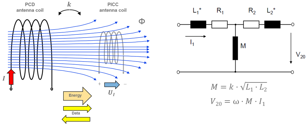
Very related to the coupling coefficient, we have the mutual inductance. The mutual inductance allows us to determine the voltage induced in the card antenna, that depends on:
- Coupling coefficient Better coupling, higher the voltage
- Driver current The higher the current we drive in the reader antenna, the stronger the magnetic field
- Antenna inductance
Precisely, in this setup, we are going to measure the voltage perceived by the reference PICC when using two different antennas.
Antenna tuning components used for the large antenna
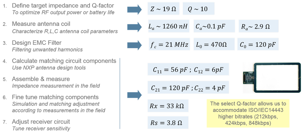
First, we prepared a tuning of 20 Ohms in the large antenna. This task was done using the process described above. As an example, we selected a low Q-factor of 10, which helped us to accommodate high bit rates for ISO14443. In the figure below, you can see the components we assembled to tune the large antenna near to 20 Ohms.
Antenna tuning components used for the small antenna
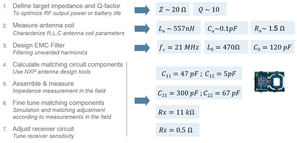
Second, we prepared a tuning of 20 Ohms in the small antenna so that the results are comparable. The same Q-factor and EMC filter values were used, but obviously, as the antenna size is different, we used different C1, C2 and Rs values to achieve the same equivalent impedance
OM29263ADK large antenna vs small antenna
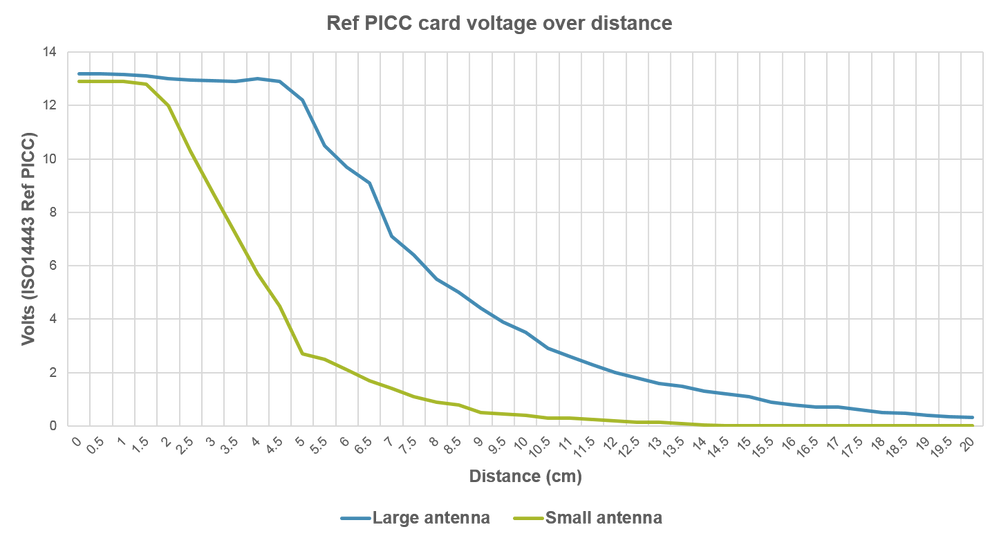
The following graph shows the results we obtained:
- The blue line, represents the DC output voltage obtained from the Class 1 Reference PICC as we increase the distance from the reader using the large antenna…
- The green line, represents the DC output voltage obtained from the Class 1 Reference PICC but using the reader with the small antenna connected.
As a result, what we see is that at close distance, both antennas are able to deliver the same field strength. However, as distance increases, the RF field of the small antenna starts to attenuate quickly from 2 cm distance of the reader while the RF field of the large antenna is more or less stable until 5 cm, after that, it starts to attenuate quickly as well. Potentially, what we can conclude is that for this setup, we might be able to get more reading distance with the large antenna.
ISO/IEC14443 vs ISO/IEC15693 reader - Quality factor
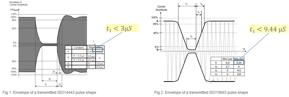
We need to bear in mind that our antenna is not only for energy transfer, but also it should match with the waveform requirements. Therefore, from the practical point of view, the Q factor of the system is limited by the bandwidth as if we increase the Q, we increase the field strength but we decrease the bandwidth. Our reader can be optimized whether we are designing a reader for ISO14443 or ISO15693 as the signals modulation and timing requirements of the rise and fall times for both RF protocols are different. Actually, in practice, ISO15693 allows us a higher Q factor because there is a lower bandwidth requirement as the waveform timings are more relaxed and, the power transfer requirement is lower than ISO14443.
For such optimization, you can refer again to NXP antenna tuning excel sheet. If you recall, one of the input fields of the excel sheet is the Q-factor. Therefore, you can introduce here a value below 30 for ISO14443 readers or below 100 for ISO15693 readers. The excel will output reasonable matching values for the first components adjustment. After that, you can do a fine tuning according to the process I explained before.
Further information
You can find more information about NFC in:
- Our NFC everywhere portal: https://www.nxp.com/nfc
- You can ask your question in our technical community: https://community.nxp.com/community/identification-security/nfc
- You can look for design partners: https://nxp.surl.ms/NFC_AEC
- And you can check our recorded training: http://www.nxp.com/support/online-academy/nfc-webinars:NFC-WEBINARS
Video recorded session
On 21 June 2018, a live session explaining this topic. You can watch the recording here:
