
- Forums
- Product Forums
- General Purpose MicrocontrollersGeneral Purpose Microcontrollers
- i.MX Forumsi.MX Forums
- QorIQ Processing PlatformsQorIQ Processing Platforms
- Identification and SecurityIdentification and Security
- Power ManagementPower Management
- Wireless ConnectivityWireless Connectivity
- RFID / NFCRFID / NFC
- Advanced AnalogAdvanced Analog
- MCX Microcontrollers
- S32G
- S32K
- S32V
- MPC5xxx
- Other NXP Products
- S12 / MagniV Microcontrollers
- Powertrain and Electrification Analog Drivers
- Sensors
- Vybrid Processors
- Digital Signal Controllers
- 8-bit Microcontrollers
- ColdFire/68K Microcontrollers and Processors
- PowerQUICC Processors
- OSBDM and TBDML
- S32M
- S32Z/E
-
- Solution Forums
- Software Forums
- MCUXpresso Software and ToolsMCUXpresso Software and Tools
- CodeWarriorCodeWarrior
- MQX Software SolutionsMQX Software Solutions
- Model-Based Design Toolbox (MBDT)Model-Based Design Toolbox (MBDT)
- FreeMASTER
- eIQ Machine Learning Software
- Embedded Software and Tools Clinic
- S32 SDK
- S32 Design Studio
- GUI Guider
- Zephyr Project
- Voice Technology
- Application Software Packs
- Secure Provisioning SDK (SPSDK)
- Processor Expert Software
- Generative AI & LLMs
-
- Topics
- Mobile Robotics - Drones and RoversMobile Robotics - Drones and Rovers
- NXP Training ContentNXP Training Content
- University ProgramsUniversity Programs
- Rapid IoT
- NXP Designs
- SafeAssure-Community
- OSS Security & Maintenance
- Using Our Community
-
- Cloud Lab Forums
-
- Knowledge Bases
- ARM Microcontrollers
- i.MX Processors
- Identification and Security
- Model-Based Design Toolbox (MBDT)
- QorIQ Processing Platforms
- S32 Automotive Processing Platform
- Wireless Connectivity
- CodeWarrior
- MCUXpresso Suite of Software and Tools
- MQX Software Solutions
- RFID / NFC
- Advanced Analog
-
- NXP Tech Blogs
- Home
- :
- MCUXpresso软件和工具
- :
- MCUXpresso IDE
- :
- Programming FRDMKL03Z board with LPC Link2 probe
Programming FRDMKL03Z board with LPC Link2 probe
Programming FRDMKL03Z board with LPC Link2 probe
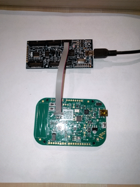
Hi, I wanted to program & debug a FRDMKL03Z board externally using LPC Link2 board from MCUXpressoIDE.
To setup I soldered two 10pin 50mil headers (J7, J8) on the FRDMKL03Z board (plus installing the SWD clock jumper J6), and confirmed the FRDMKL03Z board still continues to work on its own - with SWD clock jumper J6 closed the programming works BAU through the boards built-in P&E Micro probe/interface.
As a next step of validation I plugged the LPC Link2 board’s supplied 10pin 50mil SWD/JTAG cable between the two 10pin 50mil headers J7, J8 of the FRDMKL03Z board itself (no LPC Link2 board involved) and attempted debugging through the FRDMKL03Z board’s built in P&E Micro interface – it does not work for me with either the board’s SWD clock jumper J6 on or off. “P & E Connection Assistant” pops-up followed by an error, see bellow.
*Error captured in MCUXpressoIDE: “Error in services launch sequence
PEmicro GDB Launch Failure : The GDB Server was not able to establish a connection to the target processor. Please check your connections and power. Verify that the launch settings in the Debug Configuration are accurate.”
Looked closely for cable pin alignment, visually reexamined soldering. If it is bad soldering of the headers I would have expected the same error consistently with or without the cable, since the same signals I thought are routed internally on the board between the 10 pin headers J7, J8. Looked closer at the FRDMKL03Z board schematic, J7 & J8 which I am connecting are not routed/related. J7 is a SWD connector vs. J8 is the OPEN-SDA interface JTAG connector. Connecting the two with a cable does not make sense.
Proceeded with connecting LPC Link2 probe to FRDMKL03Z board: using the LPC Link2 supplied 10-pin cable connected LPC Link 2’s J2 connector with FRDMKL03Z board’s J7 connector. J6 jumper on FRDMKL03Z board is closed to allow SWD clock to the target MCU. J1 on LPC Link2 is open and J2 on LPC Link2 is closed (LPC Link2 powers the target FRDMKL03Z board).
Imported a gpio LED project for the FRDMKL03Z board, and proceed to build and debug it successfully with the above setup.
Thank you,
Nik
Looked closer at the FRDMKL03Z board schematic, J7 & J8 which I am connecting are not routed/related. J7 is a SWD connector vs. J8 is the OPEN-SDA interface JTAG connector. Connecting the two with a cable does not make sense.