- Forums
- Product Forums
- General Purpose MicrocontrollersGeneral Purpose Microcontrollers
- i.MX Forumsi.MX Forums
- QorIQ Processing PlatformsQorIQ Processing Platforms
- Identification and SecurityIdentification and Security
- Power ManagementPower Management
- Wireless ConnectivityWireless Connectivity
- RFID / NFCRFID / NFC
- Advanced AnalogAdvanced Analog
- MCX Microcontrollers
- S32G
- S32K
- S32V
- MPC5xxx
- Other NXP Products
- S12 / MagniV Microcontrollers
- Powertrain and Electrification Analog Drivers
- Sensors
- Vybrid Processors
- Digital Signal Controllers
- 8-bit Microcontrollers
- ColdFire/68K Microcontrollers and Processors
- PowerQUICC Processors
- OSBDM and TBDML
- S32M
- S32Z/E
-
- Solution Forums
- Software Forums
- MCUXpresso Software and ToolsMCUXpresso Software and Tools
- CodeWarriorCodeWarrior
- MQX Software SolutionsMQX Software Solutions
- Model-Based Design Toolbox (MBDT)Model-Based Design Toolbox (MBDT)
- FreeMASTER
- eIQ Machine Learning Software
- Embedded Software and Tools Clinic
- S32 SDK
- S32 Design Studio
- GUI Guider
- Zephyr Project
- Voice Technology
- Application Software Packs
- Secure Provisioning SDK (SPSDK)
- Processor Expert Software
- Generative AI & LLMs
-
- Topics
- Mobile Robotics - Drones and RoversMobile Robotics - Drones and Rovers
- NXP Training ContentNXP Training Content
- University ProgramsUniversity Programs
- Rapid IoT
- NXP Designs
- SafeAssure-Community
- OSS Security & Maintenance
- Using Our Community
-
- Cloud Lab Forums
-
- Knowledge Bases
- ARM Microcontrollers
- i.MX Processors
- Identification and Security
- Model-Based Design Toolbox (MBDT)
- QorIQ Processing Platforms
- S32 Automotive Processing Platform
- Wireless Connectivity
- CodeWarrior
- MCUXpresso Suite of Software and Tools
- MQX Software Solutions
- RFID / NFC
- Advanced Analog
-
- NXP Tech Blogs
- Home
- :
- General Purpose Microcontrollers
- :
- LPC Microcontrollers
- :
- Issue with getting UART to work. SEMIHOSTING/REDLIB?
Issue with getting UART to work. SEMIHOSTING/REDLIB?
- Subscribe to RSS Feed
- Mark Topic as New
- Mark Topic as Read
- Float this Topic for Current User
- Bookmark
- Subscribe
- Mute
- Printer Friendly Page
Issue with getting UART to work. SEMIHOSTING/REDLIB?
- Mark as New
- Bookmark
- Subscribe
- Mute
- Subscribe to RSS Feed
- Permalink
- Report Inappropriate Content
I am able to open and work with the debug UART on the LPC824 on the dev board rev C.
However when redirecting the usb uart pins RX/TX from 7 and 18 to my output pins it doesn't seem to be working. I've tied RX to TX physically and it hangs at waiting for the getLineUART(recv_buf, sizeof(recv_buf)); on the UART example code.
I think my project is messed up with the semihosting/debug/redlib stuff.
1. Is it possible to get both working at the same time?
2. What library and configuration should I be targeting to get the regular UART to work? Should I disable the debug macro's? Do I need to rewrite the code to get regular UARTs to work?
Thanks
- Mark as New
- Bookmark
- Subscribe
- Mute
- Subscribe to RSS Feed
- Permalink
- Report Inappropriate Content
Hi,
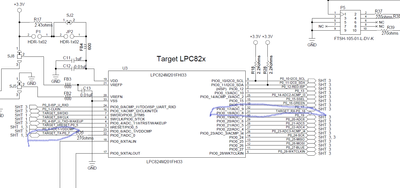
As you know that the uart0 signals can be routed to any PORT pins, on the LPC824_Xpresso board, the UART0_TX is routed to P0_7 of LPC824 as TARGET_TX-P0_7 node, then connected to PIO0_18 of UART0_RX of LPC11U35.
The UART0_RX is routed to P0_18 of LPC824 as TARGET_RX-P0_18 node, then connected to PIO0_19 of UART0_TX of LPC11U35 as node LINK_TX by closing the pin2&3 of JP3.
When the LPC824 put character to UART0_TX pin, the LPC11U35 will receive the character, then transfer it via USB to PC. The mechanism for receiver is the same.
You can route the UART0 TX/RX to the other pins via the code:
1)The code can route the UART0 pin to P0_7 and P0_18 as the example code
/* Enables clock for switch matrix.: 0x01u */
CLOCK_EnableClock(kCLOCK_Swm);
/* USART0_TXD connect to P0_7 */
SWM_SetMovablePinSelect(SWM0, kSWM_USART0_TXD, kSWM_PortPin_P0_7);
/* USART0_RXD connect to P0_18 */
SWM_SetMovablePinSelect(SWM0, kSWM_USART0_RXD, kSWM_PortPin_P0_18);
2)The code can route the UART0 pin to P0_26 and P0_25, but you have to delete the above code.
/* Enables clock for switch matrix.: 0x01u */
CLOCK_EnableClock(kCLOCK_Swm);
/* USART0_TXD connect to P0_26 */
SWM_SetMovablePinSelect(SWM0, kSWM_USART0_TXD, kSWM_PortPin_P0_26);
/* USART0_RXD connect to P0_25 */
SWM_SetMovablePinSelect(SWM0, kSWM_USART0_RXD, kSWM_PortPin_P0_25);
Pin_MUX.c
void BOARD_InitPins(void)
{
/* Enables clock for IOCON block.: 0x01u */
CLOCK_EnableClock(kCLOCK_Iocon);
/* Enables clock for switch matrix.: 0x01u */
CLOCK_EnableClock(kCLOCK_Swm);
const uint32_t pio15_config = (/* Selects pull-up function */
IOCON_PIO_MODE_PULLUP |
/* Enable hysteresis */
IOCON_PIO_HYS_EN |
/* Input not invert */
IOCON_PIO_INV_DI |
/* Disables Open-drain function */
IOCON_PIO_OD_DI |
/* Bypass input filter */
IOCON_PIO_SMODE_BYPASS |
/* IOCONCLKDIV0 */
IOCON_PIO_CLKDIV0);
/* PORT1 PIN5 (coords: ) is configured as */
IOCON_PinMuxSet(IOCON, 15, pio15_config);
const uint32_t pio30_config = (/* Selects pull-up function */
IOCON_PIO_MODE_PULLUP |
/* Enable hysteresis */
IOCON_PIO_HYS_EN |
/* Input not invert */
IOCON_PIO_INV_DI |
/* Disables Open-drain function */
IOCON_PIO_OD_DI |
/* Bypass input filter */
IOCON_PIO_SMODE_BYPASS |
/* IOCONCLKDIV0 */
IOCON_PIO_CLKDIV0);
/* PORT3 PIN0 (coords: ) is configured as */
IOCON_PinMuxSet(IOCON, 30, pio30_config);
/* USART0_TXD connect to P0_7 */
SWM_SetMovablePinSelect(SWM0, kSWM_USART0_TXD, kSWM_PortPin_P0_7);
/* USART0_RXD connect to P0_18 */
SWM_SetMovablePinSelect(SWM0, kSWM_USART0_RXD, kSWM_PortPin_P0_18);
/* Disable clock for switch matrix. */
CLOCK_DisableClock(kCLOCK_Swm);
}
Hope it can help you
BR
XiangJun Rong


