- Forums
- Product Forums
- General Purpose MicrocontrollersGeneral Purpose Microcontrollers
- i.MX Forumsi.MX Forums
- QorIQ Processing PlatformsQorIQ Processing Platforms
- Identification and SecurityIdentification and Security
- Power ManagementPower Management
- Wireless ConnectivityWireless Connectivity
- RFID / NFCRFID / NFC
- Advanced AnalogAdvanced Analog
- MCX Microcontrollers
- S32G
- S32K
- S32V
- MPC5xxx
- Other NXP Products
- S12 / MagniV Microcontrollers
- Powertrain and Electrification Analog Drivers
- Sensors
- Vybrid Processors
- Digital Signal Controllers
- 8-bit Microcontrollers
- ColdFire/68K Microcontrollers and Processors
- PowerQUICC Processors
- OSBDM and TBDML
- S32M
- S32Z/E
-
- Solution Forums
- Software Forums
- MCUXpresso Software and ToolsMCUXpresso Software and Tools
- CodeWarriorCodeWarrior
- MQX Software SolutionsMQX Software Solutions
- Model-Based Design Toolbox (MBDT)Model-Based Design Toolbox (MBDT)
- FreeMASTER
- eIQ Machine Learning Software
- Embedded Software and Tools Clinic
- S32 SDK
- S32 Design Studio
- GUI Guider
- Zephyr Project
- Voice Technology
- Application Software Packs
- Secure Provisioning SDK (SPSDK)
- Processor Expert Software
- Generative AI & LLMs
-
- Topics
- Mobile Robotics - Drones and RoversMobile Robotics - Drones and Rovers
- NXP Training ContentNXP Training Content
- University ProgramsUniversity Programs
- Rapid IoT
- NXP Designs
- SafeAssure-Community
- OSS Security & Maintenance
- Using Our Community
-
- Cloud Lab Forums
-
- Knowledge Bases
- ARM Microcontrollers
- i.MX Processors
- Identification and Security
- Model-Based Design Toolbox (MBDT)
- QorIQ Processing Platforms
- S32 Automotive Processing Platform
- Wireless Connectivity
- CodeWarrior
- MCUXpresso Suite of Software and Tools
- MQX Software Solutions
- RFID / NFC
- Advanced Analog
-
- NXP Tech Blogs
- Home
- :
- ARM Microcontrollers
- :
- Kinetis Microcontrollers Knowledge Base
- :
- Creating a gated timer using the FTM and Comparator
Creating a gated timer using the FTM and Comparator
- Subscribe to RSS Feed
- Mark as New
- Mark as Read
- Bookmark
- Subscribe
- Printer Friendly Page
- Report Inappropriate Content
Creating a gated timer using the FTM and Comparator
Creating a gated timer using the FTM and Comparator
Introduction
What is a gated timer and why would I need one?
A gated timer is a timer whose clock is enabled (or "gated") by some external signal. This allows for a low code overhead method of synchronizing a timer with an event and/or measuring an event. This functionality is not commonly included on Freescale microcontroller devices (this functionality is only included on devices that are equipped with the upgraded TPM v2 peripheral; currently K66, K65, KL13, KL23, KL33, KL43, KL03) but can be useful in some situations. Some applications which may find a gated timer useful include asynchronous digital sampling, pulse width duty cycle measurement, and battery charging.
How do I implement a gated timer with my Kinetis FTM or TPM peripheral?
To implement a true gated timer with a Kinetis device (that does not have the TPM v2 peripheral), additional hardware will be required to implement the enable/disable functionality of a gated timer. This note will focus on two different ways (low-true and high-true) to implement a gated timer. The method used will depend on the requirements of your application.
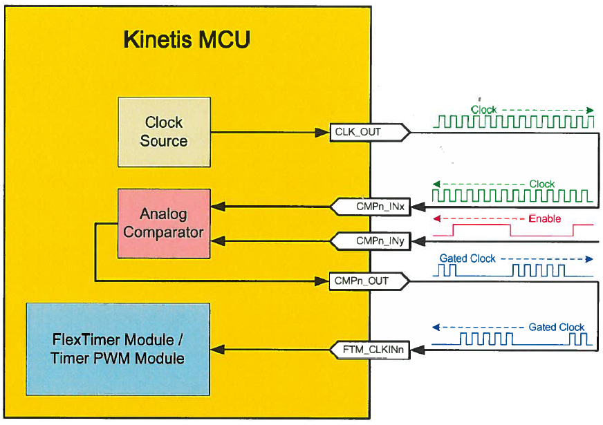
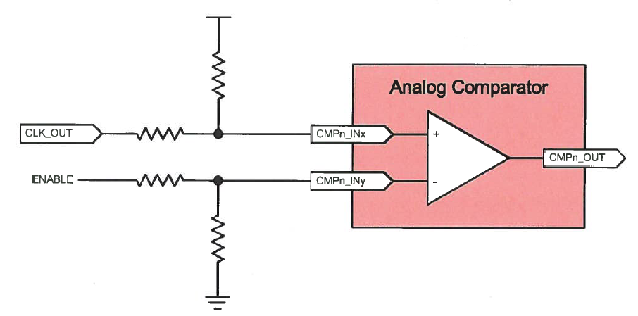
Implementing a gated timer for Kinetis devices without the TPM v2 peripheral requires the use of a comparator and a resistive network to implement a gated functionality (NOTE: Level shifters could be used to replace the resistive network described; however, a resistive network is likely more cost effective, and thus, is presented in this discussion). Figure 1 below is the block diagram of how to implement a gated timer functionality. The theory behind this configuration will be explained in later sections.
Theory of Operation
Comparator and resistive network implementation
The comparator is the key piece to implementing this functionality. For those with little experience with comparators (or need a refresher), a comparator is represented by the following figure. Notice that there are three terminals that will be of relevance in this application: a non-inverting input (labeled with a '+' sign), an inverting input (labeled with a '-' sign), and an output.
A comparator does just what the name suggests: it compares two signals and adjusts the output based on the result of the comparison. This is represented mathematically in the figure below.
Considering the above figure, output of the comparator will be a logic high when the non-inverting input is at a higher electric potential than the inverting input. The output will be a logic low if the non-inverting input is at a lower electric potential than the inverting input. The output will be unpredictable if the inputs are exactly the same (oscillations may even occur since comparators are designed to drive the output to a solid high or solid low). This mechanism allows the clock enable functionality that is required to implement a gated timer function provided that either the non-inverting or inverting input is a clock waveform and the opposite input is a stable logic high or low (depending on the desired configuration) and neither input is ever exactly equal.
Comparator Configurations
There are two basic signal configurations that an application can use to enable the clock output out of the comparator: low-true signals and high-true signals. These two signals and some details on their implementation are explained in the following two sections.
Low-true enable
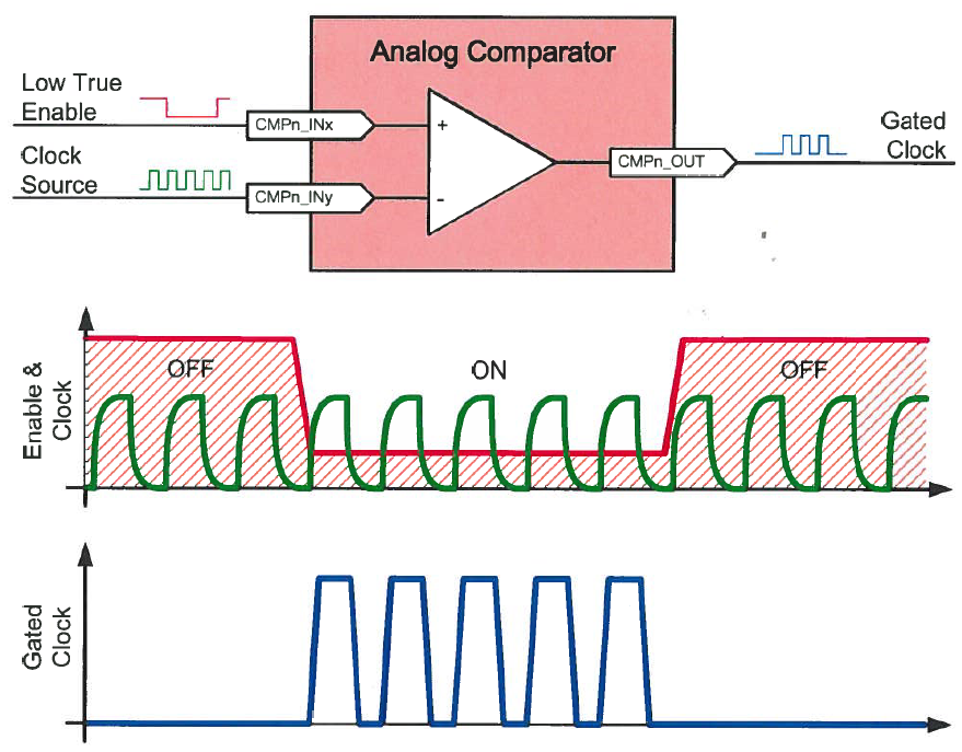
A low-true enable is an enable signal that will have zero electric potential (relative to the microcontroller) or a "grounded" signal in the "active" state. This configuration is a common implementation when using a push button or momentary switch to provide the enable signal. When using this type of signal, you will want to connect the enable signal to the non-inverting input of the comparator, and connect the clock signal to the inverting input. The high level of the enable signal should be guaranteed to always be the highest voltage of the input clock plus the maximum input offset of the comparator. To find the maximum input offset of the comparator, consult the device specific datasheet. See the figure below to see a graphical representation of areas where the signal will be on and off.
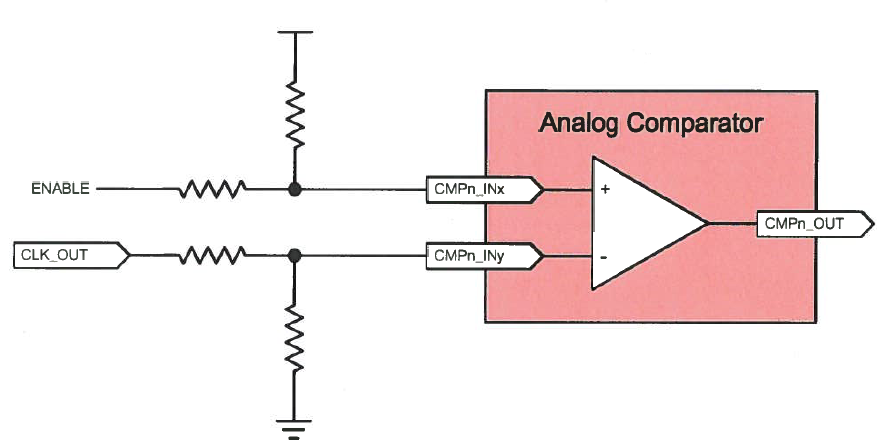
The external hardware used should ensure that the low level of the enable signal never dips below the lowest voltage of the input clock plus the maximum input offset of the comparator. The following figure displays one possible hardware configuration that is relatively inexpensive and can satisfy these requirements.
High-true enable
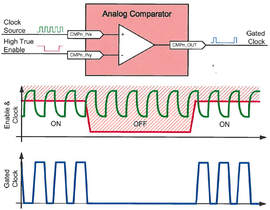
A high-true enable is an enable signal that will have an electric potential equal to VDD of the microcontroller in the "active" state. This configuration is commonly implemented when the enable signal is provided by an active source or another microcontroller. When interfacing with this type of signal, you will want to connect the enable signal to the inverting input of the comparator, and connect the clock signal to the non-inverting input. When the comparator is in the inactive state, it should be at or below the lowest voltage of the clock signal minus the maximum input offset of the comparator. Refer to the following figure for a diagram of the "on" and "off" regions of the high true configurations.
The external hardware will need to guarantee that the when the enable signal is in the active state, it does not rise above the highest voltage of the clock signal minus the maximum input offset of the comparator. The following figure displays one possible hardware configuration that is relatively inexpensive and can satisfy these requirements.
Clocking Options
Clocking waveform requirements will vary from application to application. Specifying all of the possibilities is nearly impossible. The point of this section is to inform what options are available from the Kinetis family and provide some insight as to when it might be relevant to investigate each option.
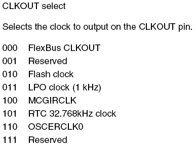
The Kinetis family provides a clock output pin for most devices to allow an internal clock to be routed to a pin. The uses for this option can vary. In this particular scenario, it will be used to provide the source clock for the comparator clock input. Here are the most common clock output pin options across the Kinetis K series devices. (NOTE: If the application requires a clock frequency that the CLKOUT signal cannot provide, a separate FTM or TPM instance or another timer module can be used to generate the required clock.)
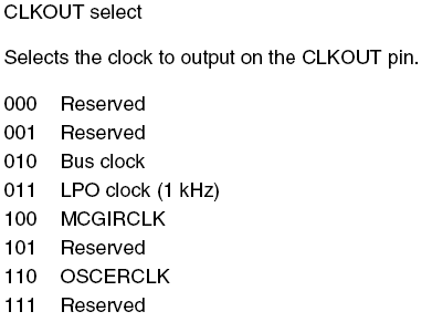
In the Kinetis L series devices, the following options will be available.
The clock option selected should be the slowest allowable clock for the application being designed. This will minimize the power consumption of the application. For applications that require high resolution, the Bus, Flash, or Flexbus clock should be selected (note that the Flexbus clock can provide an independently adjustable clock, if it is not being used in the application, as it is always running). However, if the target application needs to be more power efficient, the LPO or MCGIRCLK should be used. The LPO for the Kinetis devices is a fixed 1 kHz frequency and will, therefore, only be useful in applications that require millisecond resolutions.
