- NXP Forums
- Product Forums
- General Purpose MicrocontrollersGeneral Purpose Microcontrollers
- i.MX Forumsi.MX Forums
- QorIQ Processing PlatformsQorIQ Processing Platforms
- Identification and SecurityIdentification and Security
- Power ManagementPower Management
- MCX Microcontrollers
- S32G
- S32K
- S32V
- MPC5xxx
- Other NXP Products
- Wireless Connectivity
- S12 / MagniV Microcontrollers
- Powertrain and Electrification Analog Drivers
- Sensors
- Vybrid Processors
- Digital Signal Controllers
- 8-bit Microcontrollers
- ColdFire/68K Microcontrollers and Processors
- PowerQUICC Processors
- OSBDM and TBDML
-
- Solution Forums
- Software Forums
- MCUXpresso Software and ToolsMCUXpresso Software and Tools
- CodeWarriorCodeWarrior
- MQX Software SolutionsMQX Software Solutions
- Model-Based Design Toolbox (MBDT)Model-Based Design Toolbox (MBDT)
- FreeMASTER
- eIQ Machine Learning Software
- Embedded Software and Tools Clinic
- S32 SDK
- S32 Design Studio
- GUI Guider
- Zephyr Project
- Voice Technology
- Application Software Packs
- Secure Provisioning SDK (SPSDK)
- Processor Expert Software
-
- Topics
- Mobile Robotics - Drones and RoversMobile Robotics - Drones and Rovers
- NXP Training ContentNXP Training Content
- University ProgramsUniversity Programs
- Rapid IoT
- NXP Designs
- SafeAssure-Community
- OSS Security & Maintenance
- Using Our Community
-
- Cloud Lab Forums
-
- Home
- :
- i.MX Forums
- :
- i.MX Processors
- :
- Re: MDDR from Nanya and Micron not working on i.MX257
MDDR from Nanya and Micron not working on i.MX257
- Subscribe to RSS Feed
- Mark Topic as New
- Mark Topic as Read
- Float this Topic for Current User
- Bookmark
- Subscribe
- Mute
- Printer Friendly Page
MDDR from Nanya and Micron not working on i.MX257
- Mark as New
- Bookmark
- Subscribe
- Mute
- Subscribe to RSS Feed
- Permalink
- Report Inappropriate Content
Hello,
I am using i.MX257 processor with 256 MB(2X128MB) MDDR from Hynix “H5MS1G62BFR”. I have 25 boards that work without any issue. The board is configured to boot from SD Card.
Recently I have changed the MDDR in few board to NT6DM64M16BD-T1 from Nanya and in few other to MT46H64M16LF-6 from Micron. Though the specifications of all the three MDDR are the same the MDDRs from Nanya and Micron are not functioning.
All the three MDDRs can be operated at a maximum of 200MHz. I am operating at 133MHz because of the processor limitations.
Visual Debugging and Inspection:-
I am using U-boot 2009.08 release. All the voltages to the processor are fine. The clko pin of the processor provide 8.19KHz. In dcdheader.S, when I change the clock to the memory to 100MHz, I see the same frequency while probing the sdclk(memory clock) line. But changing the same in lowlevel_init.S, I do not find any change in the frequency. Does this mean my U-boot is not booting after relocating to the MDDR? Why is this happening ?
Results when running in ATK mode:-
BOOT_MODE[1:0] were configured as “11”. The running ATK program provided by Freescale, I was able to download my u boot to 0X80004000 and also flash my SD card. Does this mean that I was able to write to my MDDR and read from the same ? If yes then why is my U-boot not booting up?
Debugging through JTAG interface:-
Using Amontec JTAG with OpenOCD I tested the MDDR. Surprisingly I was able to access all the memory locations. Using “runAllMemTests “ command I was able to test my entire 256MB of RAM.
The timing parameters were the same as I used in my U-boot(dcdheader.S). So there is no issues in assembling and soldering, then why is my U-boot is not booting ?
Also I used gdb to debug the U-boot; being new to gdb I followed the steps mentioned in http://www.denx.de/wiki/view/DULG/DebuggingUBoot. I could not locate where is “cpu_init.c” to insert a breakpoint, so I continued to which the JTAG prompt threw “memory read caused data abort (address: 0x80f00500, size: 0x4, count: 0x1) “ . On checking the map file I found that this address points to cpu/arm926ejs/start.o.
The above mentioned results is common for both Nanya and Micron MDDRs. But I do not see this issue in Hynix. Also in few boards I replaced the Nanya and Micron with the older re-balled Hynix; even those boards are booting up.
The source code of u-boot is similar to http://git.freescale.com/git/cgit.cgi/imx/uboot-imx.git/tree/?h=imx_v2009.08
Please let me know if my steps in debugging are wrong, is there something more I need to do to get these MDDRs working. Why am I able to access the RAM in JTAG. Is this issue related to PCB routing, or the U-boot, or these MDDRs or the Memory controller in i.MX257.
Thanking You,
Harsha
- Mark as New
- Bookmark
- Subscribe
- Mute
- Subscribe to RSS Feed
- Permalink
- Report Inappropriate Content
HI Harsha
this may be caused by non-optimal drive sterngth (for example faster grades memories
produce more noise), one can tweak it both from i.MX25 side and from DDR
(using write to mode register).
Varying temperature (for example wiith cooling spray) is one method to narrow
down the root cause:
- If cooling down the part causes more failures, then it is likely the drive strength
is too high causing more overshoots and undershoots
- If heating up the part causes more failures, then the drive strength is too low a
nd the signals may not rise/fall fast enough
it is recommended to run memory test with jtag debugger (you can create service request
and obtain simple test), also it isrecommended to look at mDDR_init.zip
Re: how to configure LPDDR on i.MX257
Best regards
igor
-----------------------------------------------------------------------------------------------------------------------
Note: If this post answers your question, please click the Correct Answer button. Thank you!
-----------------------------------------------------------------------------------------------------------------------
- Mark as New
- Bookmark
- Subscribe
- Mute
- Subscribe to RSS Feed
- Permalink
- Report Inappropriate Content
Hello Igor,
Thanks for the reply.
I did change the drive strengths through the EMR registers, DCDGEN(18, 1, 0x81000020, 0xff) --half drive strenght and DCDGEN(18, 1, 0x81000030, 0xff) quarter drive strength. I see the same amount of overshoot and undershoot when I probe all my 3 MDDRs. But only when I drive it full strength the Hynix based board boots up, but not the Micron or Nanya based.
The datasheet to the Hynix is here http://www.farnell.com/datasheets/1641686.pdf
The datasheet to the Micron is http://www.dinigroup.com/files/1gb_ddr_mobile_sdram_t48m.pdf
My DDR settings are similar to the one suggested by you, below you can see the dcdheader contents-
#include <config.h>
#include <version.h>
..extern reset
#define DCDGEN(i,type, addr, data) \
dcd_##i:
.long type
.long addr
.long data
..globl _initheader
_initheader:
b reset
.org 0x400
app_code_jump_v: .long reset
app_code_barker: .long 0xB1
app_code_csf: .long 0
hwcfg_ptr_ptr: .long hwcfg_ptr
super_root_key: .long 0
hwcfg_ptr: .long dcd_data
app_dest_ptr: .long TEXT_BASE
dcd_data: .long 0xB17219E9
dcd_len: .long 12*25
/* Remove WEIM init */
/* WEIM config-CS5 init -- CPLD */
DCDGEN( 1, 4, 0xB8002050, 0x0000D843) /* CS5_CSCRU */
DCDGEN( 2, 4, 0xB8002054, 0x22252521) /* CS5_CSCRL */
DCDGEN( 3, 4, 0xB8002058, 0x22220A00) /* CS5_CSCRA */
/* MDDR init -- original*/
DCDGEN( 4, 4, 0xB8001010, 0x00000004) /* enable mDDR */
DCDGEN( 5, 4, 0xB8001000, 0x93200000) /* precharge command --14 rows 10 coloumns*/
DCDGEN( 6, 4, 0xB8001008, 0x93200000) /* precharge command */
DCDGEN( 7, 1, 0x80000400, 0x12344321) /* precharge all dummy write */
DCDGEN( 8, 1, 0x90000400, 0x12344321) /* precharge all dummy write */
DCDGEN( 9, 4, 0xB8001000, 0xA3200000) /* auto-refresh command */
DCDGEN(10, 4, 0xB8001008, 0xA3200000) /* auto-refresh command */
DCDGEN(11, 4, 0x80000000, 0x12344321) /* dummy write for refresh */
DCDGEN(12, 4, 0x80000000, 0x12344321) /* dummy write for refresh */
DCDGEN(13, 4, 0x90000000, 0x12344321) /* dummy write for refresh */
DCDGEN(14, 4, 0x90000000, 0x12344321) /* dummy write for refresh */
DCDGEN(15, 4, 0xB8001000, 0xB3200000) /* Load Mode Reg command - cas=3 bl=8 */
DCDGEN(16, 4, 0xB8001008, 0xB3200000) /* Load Mode Reg command - cas=3 bl=8 */
DCDGEN(17, 1, 0x80000033, 0xda) /* dummy write -- address has the mode bits */
DCDGEN(18, 1, 0x81000000, 0xff) /* dummy write -- address has the mode bits */
DCDGEN(19, 1, 0x90000033, 0xda) /* dummy write -- address has the mode bits */
DCDGEN(20, 1, 0x91000000, 0xff) /* dummy write -- address has the mode bits */
DCDGEN(21, 4, 0xB8001000, 0x83216880) /* aligned to D[15:0],7.81uS refresh rate, PRCT disabled PWDT=64HCLK */
DCDGEN(22, 4, 0xB8001008, 0x83216880) /* Burst length not set to full page, Burst length 8 */
DCDGEN(23, 4, 0xB8001004, 0x00395729) /* according to datasheet */
DCDGEN(24, 4, 0xB800100C, 0x00395729)
DCDGEN(99, 4, 0x53F80008, 0x20034000) /* CLKCTL ARM=400 AHB=133 */
card_cfg: .long UBOOT_IMAGE_SIZE
How am I able to read and write the RAM locations via the JTAG interface for the above timing and configuration settings? I will create a service request and update you very soon.
Regards,
Harsha
- Mark as New
- Bookmark
- Subscribe
- Mute
- Subscribe to RSS Feed
- Permalink
- Report Inappropriate Content
HI Harsha
one can also tweak drive strength from i.MX25 side with
4.3.2 Software Pad Group Control Registers (SW_PAD_CTL_GRP) IMX25RM
and set all values in ESDCFG0 register (sect.24.3.3.2) to max. values
Best regards
igor
- Mark as New
- Bookmark
- Subscribe
- Mute
- Subscribe to RSS Feed
- Permalink
- Report Inappropriate Content
Hello Igor,
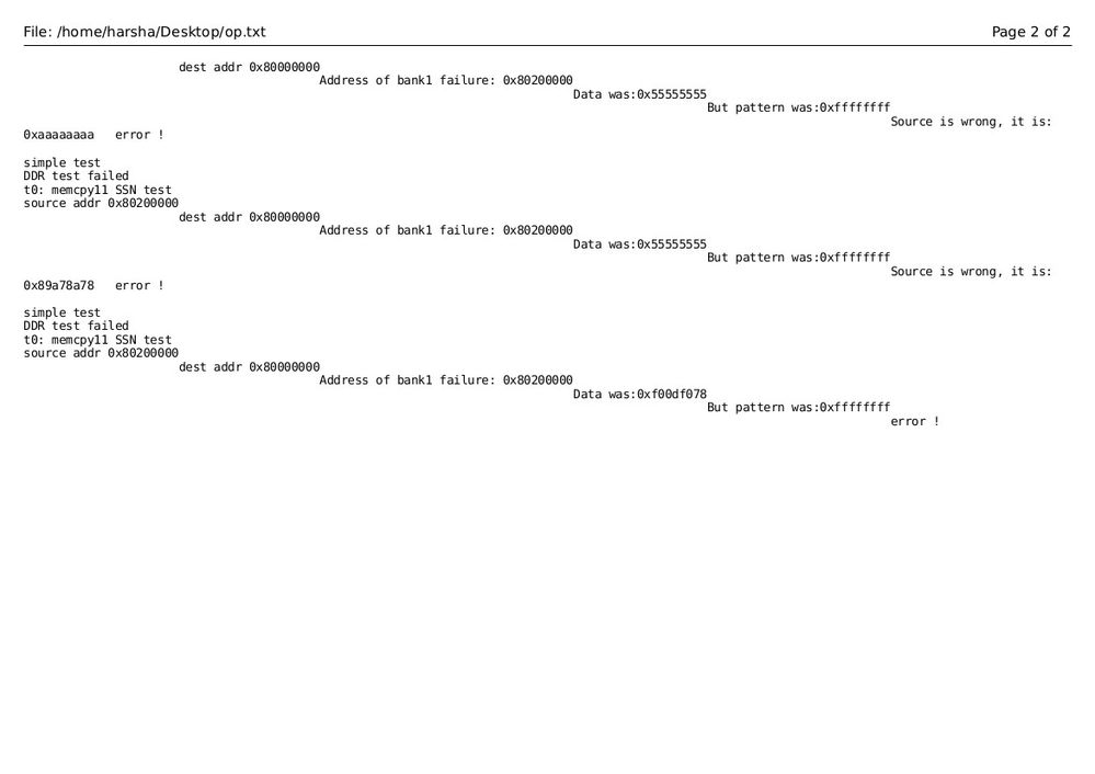
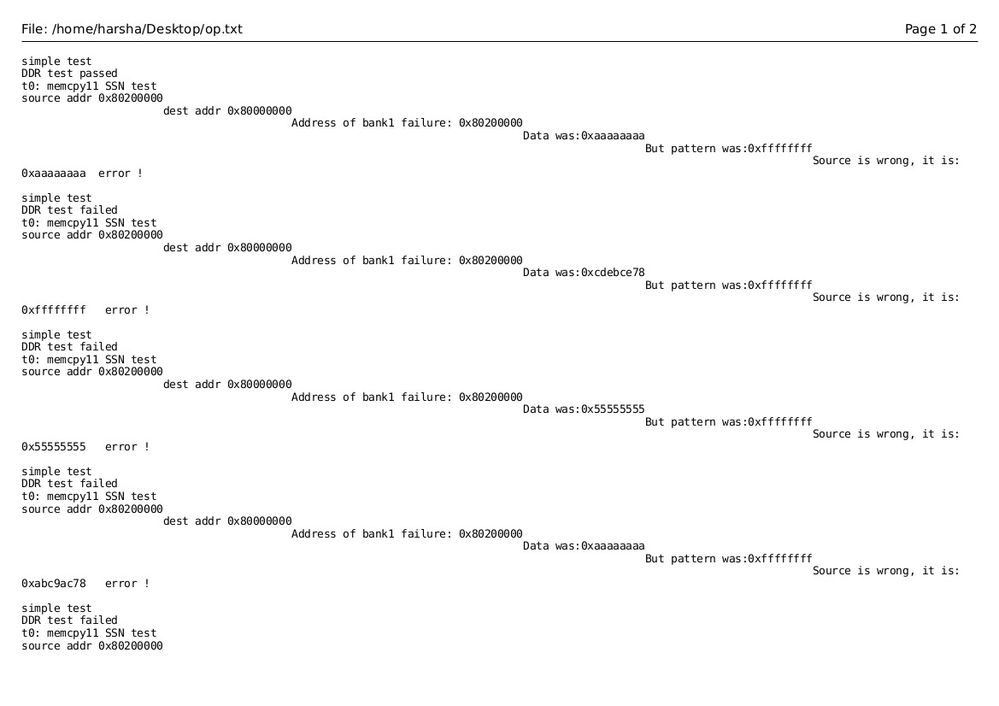
I got the test programs from Freescale Support. On running them on my boards eith Hynix MDDR, it passed all the tests. But for Nanya only the "ddr_test" passes remaining SSN based tests fail i.e( "DDRtest_memcpy11_SSN", "DDRtest_SSN_memcpy_test", "DDRtest_memcpy11_pseudo_random_with_offset" and "DDRtest_byte_SSN_test").
The output of "DDRtest_memcpy11_SSN" is attached in this mail.

As suggested by you in the previous answers I started changin the drive strength in the MDDR end. 
Regards,
Harsha.M
- Mark as New
- Bookmark
- Subscribe
- Mute
- Subscribe to RSS Feed
- Permalink
- Report Inappropriate Content
HI Harsha
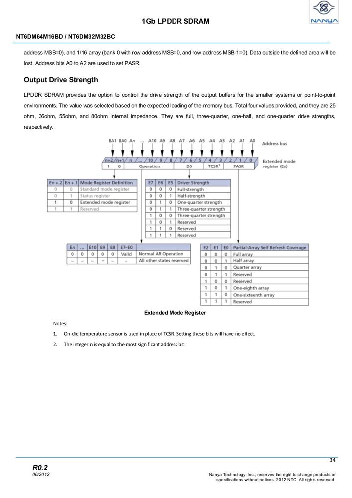
regarding "reserved" settings meaning, I think
you needs to ask vendor of that ddr part.
Best regards
igor
- Mark as New
- Bookmark
- Subscribe
- Mute
- Subscribe to RSS Feed
- Permalink
- Report Inappropriate Content
Hello Igor,
I guess my question was not sentenced well. The setting of "100" was under the field "DS" of EMR. Bit 7,6,5. so the value of EMR is 0X81000080.
Regards,
Harsha.M
- Mark as New
- Bookmark
- Subscribe
- Mute
- Subscribe to RSS Feed
- Permalink
- Report Inappropriate Content
HI Harsha
I can not comment on non-Freescale document, I think
you needs to ask vendor of that ddr part.
Also suggest to check by oscilloscope what actual value is
written on EMR.
Best regards
igor
