- NXP Forums
- Product Forums
- General Purpose MicrocontrollersGeneral Purpose Microcontrollers
- i.MX Forumsi.MX Forums
- QorIQ Processing PlatformsQorIQ Processing Platforms
- Identification and SecurityIdentification and Security
- Power ManagementPower Management
- MCX Microcontrollers
- S32G
- S32K
- S32V
- MPC5xxx
- Other NXP Products
- Wireless Connectivity
- S12 / MagniV Microcontrollers
- Powertrain and Electrification Analog Drivers
- Sensors
- Vybrid Processors
- Digital Signal Controllers
- 8-bit Microcontrollers
- ColdFire/68K Microcontrollers and Processors
- PowerQUICC Processors
- OSBDM and TBDML
-
- Solution Forums
- Software Forums
- MCUXpresso Software and ToolsMCUXpresso Software and Tools
- CodeWarriorCodeWarrior
- MQX Software SolutionsMQX Software Solutions
- Model-Based Design Toolbox (MBDT)Model-Based Design Toolbox (MBDT)
- FreeMASTER
- eIQ Machine Learning Software
- Embedded Software and Tools Clinic
- S32 SDK
- S32 Design Studio
- Vigiles
- GUI Guider
- Zephyr Project
- Voice Technology
- Application Software Packs
- Secure Provisioning SDK (SPSDK)
- Processor Expert Software
-
- Topics
- Mobile Robotics - Drones and RoversMobile Robotics - Drones and Rovers
- NXP Training ContentNXP Training Content
- University ProgramsUniversity Programs
- Rapid IoT
- NXP Designs
- SafeAssure-Community
- OSS Security & Maintenance
- Using Our Community
-
- Cloud Lab Forums
-
- Home
- :
- i.MX Forums
- :
- i.MX RT Knowledge Base
- :
- RT10XX RT-UFL modification for QSPI QE and DQS factor
RT10XX RT-UFL modification for QSPI QE and DQS factor
- Subscribe to RSS Feed
- Mark as New
- Mark as Read
- Bookmark
- Subscribe
- Printer Friendly Page
- Report Inappropriate Content
RT10XX RT-UFL modification for QSPI QE and DQS factor
RT10XX RT-UFL modification for QSPI QE and DQS factor
RT10XX RT-UFL modification for QSPI QE and DQS factor
1. Abstract
Recently, a customer used a QSPI flash (Puya simi P25Q16H) as XIP memory in the RT1050 project, but always encountered the phenomenon that the first time download failed, the download succeeded again after powering on again, and the app could run. To the program algorithm, they use the RT-UFL. After analysis, this situation is usually related to the fact that the QE of the new QSPI flash is not enabled. Therefore, based on the QE position of the QSPI flash used by the customer, the author specially enabled the corresponding QE in the SDK flexspi_nor_polling_transfer code, let the customer try to run it in RAM to check whether still have the program issues after enabling QE in the new QSPI flash. However, the customer even can’t run flexspi_nor_polling_transfer project. According to the customer's previous description, the hardware can run RAM code, and the first flash download does not work, but it can run after re-downloading, so the hardware works. Based on the phenomenon, it is initially speculated that the new problem may be related to FlexSPI DQS being occupied. Under normal circumstances, it is recommended to leave FlexSPI DQS floating. Because the project flexSPI frequency given to customers is 120Mhz, if DQS is used, the internal sampling clock source of FlexSPI read data is: Read strobe provided by memory device and input from DQS pad. This method will have problems. So asked the customer to confirm the hardware again. The result is DQS is used as a control pin for other circuits on the customer's board. Usually there are two points to note in this situation:
First, the FlexSPI clock is controlled within 60MHz.
Second, the internal sampling clock source configuration of FlexSPI read data is: Dummy read strobe generated by FlexSPI controller and looped back internally (FlexSPIn_MCR0[RXCLKSRC] = 0x0)
Therefore, this article focuses on how to prepare the test code for the corresponding QE position based on the QSPI flash used by the customer, consider the operation when DQS is enabled, modify and test the RT-UFL downloading algorithm.
2. Hardware and software prepare
To reproduce the customer issues, need to prepare the related software, hardware, and the flash programming flashdriver, and the code for testing the QE situation.
2.1 Hardware prepare
MIMXRT1050-EVKB, modify the on board resistor, from the default hyperflash to QSPI flash. The modification points:
USE QSPI FLASH(Mount R153~R158, DNP R356,R361~R366)。
Remove the on board U33 ISSI QSPI flash, burn the new QSPI flash with customer used Puya simi P25Q16H.
Customer is using JLINK, so prepare JLINK plus for downloading.
2.2 flexspi_nor_polling_transfer software prepare
SDK2.14.0 code:flexspi_nor_polling_transfer, used to test the QE situation.
App project: led_blinky
RT-UFL program algorithm code: https://github.com/JayHeng/RT-UFL
JLINK driver: used JLINKV768B, higher version is also OK.
2.2.1 P25Q16H QE position
Fig 1
We can see, it is still the typical Status register bit 9.
The related LUT write and read commander is:
Fig 2
We can see that for writing, it is command 0X01, and 2 consecutive bytes need to be written. But for the read command, the commands for the two status register bytes are separate. So you need to pay attention to this when operating the QE bit.
2.2.2 flexspi_nor_polling_transfer code prepare
This code is mainly used to test the QE enablement and disabling, and the erase, write and read functions of external flash.
The code modification points include: modifying the LUT command to comply with P25Q16H; adding QE read, write and erase functions; modifying the frequency of flexSPI and the situation of DQS loopback internal.
The relevant code is as follows:
LUT related commander: flexspi_nor_polling_transfer.c
const uint32_t customLUT[CUSTOM_LUT_LENGTH] = {
    /* Normal read mode -SDR */
    [4 * NOR_CMD_LUT_SEQ_IDX_READ_NORMAL] =
        FLEXSPI_LUT_SEQ(kFLEXSPI_Command_SDR, kFLEXSPI_1PAD, 0x03, kFLEXSPI_Command_RADDR_SDR, kFLEXSPI_1PAD, 0x18),
    [4 * NOR_CMD_LUT_SEQ_IDX_READ_NORMAL + 1] =
        FLEXSPI_LUT_SEQ(kFLEXSPI_Command_READ_SDR, kFLEXSPI_1PAD, 0x04, kFLEXSPI_Command_STOP, kFLEXSPI_1PAD, 0),

    /* Fast read mode - SDR */
    [4 * NOR_CMD_LUT_SEQ_IDX_READ_FAST] =
        FLEXSPI_LUT_SEQ(kFLEXSPI_Command_SDR, kFLEXSPI_1PAD, 0x0B, kFLEXSPI_Command_RADDR_SDR, kFLEXSPI_1PAD, 0x18),
    [4 * NOR_CMD_LUT_SEQ_IDX_READ_FAST + 1] = FLEXSPI_LUT_SEQ(
        kFLEXSPI_Command_DUMMY_SDR, kFLEXSPI_1PAD, 0x08, kFLEXSPI_Command_READ_SDR, kFLEXSPI_1PAD, 0x04),

    /* Fast read quad mode - SDR */
    [4 * NOR_CMD_LUT_SEQ_IDX_READ_FAST_QUAD] =
        FLEXSPI_LUT_SEQ(kFLEXSPI_Command_SDR, kFLEXSPI_1PAD, 0xEB, kFLEXSPI_Command_RADDR_SDR, kFLEXSPI_4PAD, 0x18),
    [4 * NOR_CMD_LUT_SEQ_IDX_READ_FAST_QUAD + 1] = FLEXSPI_LUT_SEQ(
        kFLEXSPI_Command_DUMMY_SDR, kFLEXSPI_4PAD, 0x06, kFLEXSPI_Command_READ_SDR, kFLEXSPI_4PAD, 0x04),

    /* Read extend parameters */
    [4 * NOR_CMD_LUT_SEQ_IDX_READSTATUS] =
        FLEXSPI_LUT_SEQ(kFLEXSPI_Command_SDR, kFLEXSPI_1PAD, 0x81, kFLEXSPI_Command_READ_SDR, kFLEXSPI_1PAD, 0x04),

    /* Write Enable */
    [4 * NOR_CMD_LUT_SEQ_IDX_WRITEENABLE] =
        FLEXSPI_LUT_SEQ(kFLEXSPI_Command_SDR, kFLEXSPI_1PAD, 0x06, kFLEXSPI_Command_STOP, kFLEXSPI_1PAD, 0),

    /* Erase Sector  */
    [4 * NOR_CMD_LUT_SEQ_IDX_ERASESECTOR] =
        FLEXSPI_LUT_SEQ(kFLEXSPI_Command_SDR, kFLEXSPI_1PAD, 0x20, kFLEXSPI_Command_RADDR_SDR, kFLEXSPI_1PAD, 0x18),//0xD7

    /* Page Program - single mode */
    [4 * NOR_CMD_LUT_SEQ_IDX_PAGEPROGRAM_SINGLE] =
        FLEXSPI_LUT_SEQ(kFLEXSPI_Command_SDR, kFLEXSPI_1PAD, 0x02, kFLEXSPI_Command_RADDR_SDR, kFLEXSPI_1PAD, 0x18),
    [4 * NOR_CMD_LUT_SEQ_IDX_PAGEPROGRAM_SINGLE + 1] =
        FLEXSPI_LUT_SEQ(kFLEXSPI_Command_WRITE_SDR, kFLEXSPI_1PAD, 0x04, kFLEXSPI_Command_STOP, kFLEXSPI_1PAD, 0),

    /* Page Program - quad mode */
    [4 * NOR_CMD_LUT_SEQ_IDX_PAGEPROGRAM_QUAD] =
        FLEXSPI_LUT_SEQ(kFLEXSPI_Command_SDR, kFLEXSPI_1PAD, 0x32, kFLEXSPI_Command_RADDR_SDR, kFLEXSPI_1PAD, 0x18),
    [4 * NOR_CMD_LUT_SEQ_IDX_PAGEPROGRAM_QUAD + 1] =
        FLEXSPI_LUT_SEQ(kFLEXSPI_Command_WRITE_SDR, kFLEXSPI_4PAD, 0x04, kFLEXSPI_Command_STOP, kFLEXSPI_1PAD, 0),

    /* Read ID */
    [4 * NOR_CMD_LUT_SEQ_IDX_READID] =
        FLEXSPI_LUT_SEQ(kFLEXSPI_Command_SDR, kFLEXSPI_1PAD, 0x9F, kFLEXSPI_Command_READ_SDR, kFLEXSPI_1PAD, 0x04),

    /* Enable Quad mode */
    [4 * NOR_CMD_LUT_SEQ_IDX_WRITESTATUSREG] =
        FLEXSPI_LUT_SEQ(kFLEXSPI_Command_SDR, kFLEXSPI_1PAD, 0x01, kFLEXSPI_Command_WRITE_SDR, kFLEXSPI_1PAD, 0x04),

    /* Enter QPI mode */
    [4 * NOR_CMD_LUT_SEQ_IDX_ENTERQPI] =
        FLEXSPI_LUT_SEQ(kFLEXSPI_Command_SDR, kFLEXSPI_1PAD, 0x35, kFLEXSPI_Command_STOP, kFLEXSPI_1PAD, 0),

    /* Exit QPI mode */
    [4 * NOR_CMD_LUT_SEQ_IDX_EXITQPI] =
        FLEXSPI_LUT_SEQ(kFLEXSPI_Command_SDR, kFLEXSPI_4PAD, 0xF5, kFLEXSPI_Command_STOP, kFLEXSPI_1PAD, 0),

    /* Read status register */
    [4 * NOR_CMD_LUT_SEQ_IDX_READSTATUSREG] =
        FLEXSPI_LUT_SEQ(kFLEXSPI_Command_SDR, kFLEXSPI_1PAD, 0x05, kFLEXSPI_Command_READ_SDR, kFLEXSPI_1PAD, 0x04),

	    /* Read status register */
	[4 * NOR_CMD_LUT_SEQ_IDX_READSTATUSREG1] =
	     FLEXSPI_LUT_SEQ(kFLEXSPI_Command_SDR, kFLEXSPI_1PAD, 0x35, kFLEXSPI_Command_READ_SDR, kFLEXSPI_1PAD, 0x04),

    /* Erase whole chip */
    [4 * NOR_CMD_LUT_SEQ_IDX_ERASECHIP] =
        FLEXSPI_LUT_SEQ(kFLEXSPI_Command_SDR, kFLEXSPI_1PAD, 0xC7, kFLEXSPI_Command_STOP, kFLEXSPI_1PAD, 0),//0xC7
};
flexspi_nor_flash_ops.c: QE read and write
status_t flexspi_nor_enable_quad_mode(FLEXSPI_Type *base)
{
    flexspi_transfer_t flashXfer;
    status_t status;
    uint32_t writeValue = FLASH_QUAD_ENABLE;

#if defined(CACHE_MAINTAIN) && CACHE_MAINTAIN
    flexspi_cache_status_t cacheStatus;
    flexspi_nor_disable_cache(&cacheStatus);
#endif

    /* Write enable */
    status = flexspi_nor_write_enable(base, 0);

    if (status != kStatus_Success)
    {
        return status;
    }

    /* Enable quad mode. */
    flashXfer.deviceAddress = 0;
    flashXfer.port          = FLASH_PORT;
    flashXfer.cmdType       = kFLEXSPI_Write;
    flashXfer.SeqNumber     = 1;
    flashXfer.seqIndex      = NOR_CMD_LUT_SEQ_IDX_WRITESTATUSREG;
    flashXfer.data          = &writeValue;
    flashXfer.dataSize      = writeValue <= 0xFFU ? 1 : 2;

    status = FLEXSPI_TransferBlocking(base, &flashXfer);
    if (status != kStatus_Success)
    {
        return status;
    }

    status = flexspi_nor_wait_bus_busy(base);

    /* Do software reset. */
    FLEXSPI_SoftwareReset(base);

#if defined(CACHE_MAINTAIN) && CACHE_MAINTAIN
    flexspi_nor_enable_cache(cacheStatus);
#endif

    return status;
}

status_t flexspi_nor_disable_quad_mode(FLEXSPI_Type *base)
{
    flexspi_transfer_t flashXfer;
    status_t status;
    uint32_t writeValue = 0x0;//FLASH_QUAD_ENABLE;

#if defined(CACHE_MAINTAIN) && CACHE_MAINTAIN
    flexspi_cache_status_t cacheStatus;
    flexspi_nor_disable_cache(&cacheStatus);
#endif

    /* Write enable */
    status = flexspi_nor_write_enable(base, 0);

    if (status != kStatus_Success)
    {
        return status;
    }

    /* Enable quad mode. */
    flashXfer.deviceAddress = 0;
    flashXfer.port          = FLASH_PORT;
    flashXfer.cmdType       = kFLEXSPI_Write;
    flashXfer.SeqNumber     = 1;
    flashXfer.seqIndex      = NOR_CMD_LUT_SEQ_IDX_WRITESTATUSREG;
    flashXfer.data          = &writeValue;
    flashXfer.dataSize      = 2;

    status = FLEXSPI_TransferBlocking(base, &flashXfer);
    if (status != kStatus_Success)
    {
        return status;
    }

    status = flexspi_nor_wait_bus_busy(base);

    /* Do software reset. */
    FLEXSPI_SoftwareReset(base);

#if defined(CACHE_MAINTAIN) && CACHE_MAINTAIN
    flexspi_nor_enable_cache(cacheStatus);
#endif

    return status;
}

status_t flexspi_nor_QE_register(FLEXSPI_Type *base, uint32_t *QEvalue)
{
    /* Wait status ready. */
    bool isBusy;
    uint32_t readValue;
    status_t status;
    flexspi_transfer_t flashXfer;

    flashXfer.deviceAddress = 0;
    flashXfer.port          = FLASH_PORT;
    flashXfer.cmdType       = kFLEXSPI_Read;
    flashXfer.SeqNumber     = 1;
    flashXfer.seqIndex      = NOR_CMD_LUT_SEQ_IDX_READSTATUSREG1;
    flashXfer.data          = &readValue;
    flashXfer.dataSize      = 1;

    do
    {
        status = FLEXSPI_TransferBlocking(base, &flashXfer);

        if (status != kStatus_Success)
        {
            return status;
        }
        if (FLASH_BUSY_STATUS_POL)
        {
            if (readValue & (1U << FLASH_BUSY_STATUS_OFFSET))
            {
                isBusy = true;
            }
            else
            {
                isBusy = false;
            }
        }
        else
        {
            if (readValue & (1U << FLASH_BUSY_STATUS_OFFSET))
            {
                isBusy = false;
            }
            else
            {
                isBusy = true;
            }
        }
        *QEvalue = readValue;

    } while (isBusy);

    return status;
}
QE position:App.h
#define FLASH_QUAD_ENABLE 0X0200QE operation:flexspi_nor_polling_transfer.c
 PRINTF("Get the QE bit value before QE enable!\r\n");
    uint32_t QEvalue=0;
    status = flexspi_nor_QE_register(EXAMPLE_FLEXSPI, &QEvalue);
    if (status != kStatus_Success)
    {
        return status;
    }
    PRINTF("QE=%X!\r\n",(uint8_t)QEvalue);
#if 1
    status = flexspi_nor_disable_quad_mode(EXAMPLE_FLEXSPI);
    if (status != kStatus_Success)
    {
        return status;
    }
    PRINTF("Get the QE bit value after QE disable!\r\n");

   status = flexspi_nor_QE_register(EXAMPLE_FLEXSPI, &QEvalue);
   if (status != kStatus_Success)
   {
       return status;
   }
   PRINTF("QE=%X!\r\n",(uint8_t)QEvalue);
#endif

   PRINTF("Enable the QE bit value !\r\n");
    /* Enter quad mode. */
    status = flexspi_nor_enable_quad_mode(EXAMPLE_FLEXSPI);
    if (status != kStatus_Success)
    {
        return status;
    }

    status = flexspi_nor_QE_register(EXAMPLE_FLEXSPI, &QEvalue);
    if (status != kStatus_Success)
    {
        return status;
    }
    PRINTF("QE=%X!\r\n",(uint8_t)QEvalue);
FlexSPI frequency modification:flexspi_nor_polling_transfer.c,app.h
flexspi_device_config_t deviceconfig = {
    .flexspiRootClk       = 60000000,
    .flashSize            = FLASH_SIZE,
    .CSIntervalUnit       = kFLEXSPI_CsIntervalUnit1SckCycle,
    .CSInterval           = 2,
    .CSHoldTime           = 3,
    .CSSetupTime          = 3,
    .dataValidTime        = 0,
    .columnspace          = 0,
    .enableWordAddress    = 0,
    .AWRSeqIndex          = 0,
    .AWRSeqNumber         = 0,
    .ARDSeqIndex          = NOR_CMD_LUT_SEQ_IDX_READ_FAST_QUAD,
    .ARDSeqNumber         = 1,
    .AHBWriteWaitUnit     = kFLEXSPI_AhbWriteWaitUnit2AhbCycle,
    .AHBWriteWaitInterval = 0,
};
static inline void flexspi_clock_init(void)
{
    const clock_usb_pll_config_t g_ccmConfigUsbPll = {.loopDivider = 0U};

    CLOCK_InitUsb1Pll(&g_ccmConfigUsbPll);
    CLOCK_InitUsb1Pfd(kCLOCK_Pfd0, 24);   /* Set PLL3 PFD0 clock 360MHZ. */
    CLOCK_SetMux(kCLOCK_FlexspiMux, 0x3); /* Choose PLL3 PFD0 clock as flexspi source clock. */
    CLOCK_SetDiv(kCLOCK_FlexspiDiv, 5);   /* flexspi clock 60M. */
}
Loop back internally:app.h
#define EXAMPLE_FLEXSPI_RX_SAMPLE_CLOCK kFLEXSPI_ReadSampleClkLoopbackInternally 2.2.3 flexspi_nor_polling_transfer testing after modification
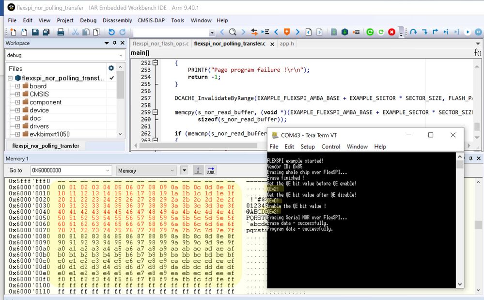
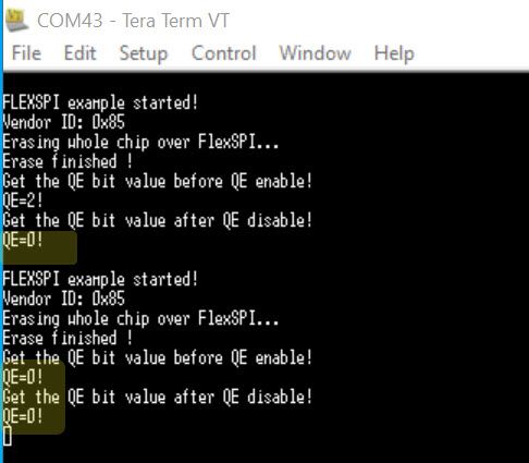
Download the modified code to RT1050 RAM and run the results as follows:
Fig 3
From the figure, we can see, QE can normally implement the functions of reading, writing, erasing, and reading. It is read as 2 here which QE is enabled for the first time, because the QSPI in this article has been operated previously. If it is a new chip, it will read 0 by default, which means that QE is not enabled. And it can be seen that after modification, it can accurately erase, program, and read external flash, indicating that the current code modification is successful. LUT, QE position, DQS consideration (60Mhz+loopback internal) are all working.
2.3 APP prepare
Use the led_blinky code in the SDK to mainly modify the frequency of FCB and readSampleClkSrc.
evkbimxrt1050_flexspi_nor_config.c is modified as follows:
const flexspi_nor_config_t qspiflash_config = {
    .memConfig =
        {
            .tag                  = FLEXSPI_CFG_BLK_TAG,
            .version              = FLEXSPI_CFG_BLK_VERSION,
            .readSampleClksrc=kFlexSPIReadSampleClk_LoopbackInternally,
            .csHoldTime           = 3u,
            .csSetupTime          = 3u,
            .controllerMiscOption = (1u << kFlexSpiMiscOffset_SafeConfigFreqEnable),
            .deviceType           = kFlexSpiDeviceType_SerialNOR,
            .sflashPadType        = kSerialFlash_4Pads,
            .serialClkFreq        = kFlexSpiSerialClk_60MHz,
            .sflashA1Size         = 8u * 1024u * 1024u,
…
}
This code will be used to test the new modified program flashdriver in debug mode, compile the project, generate the .srec, used for the JFLASH method flash program.
3. RT-UFL JLINK flash algorithm modification
After downloading the super download algorithm RT-UFL, you need to modify the super download algorithm based on the two factors mentioned above:
First, QE is enabled; second, DQS is used.
For the solution in this article, RT-UFL still uses option ROM to initialize flexSPI.
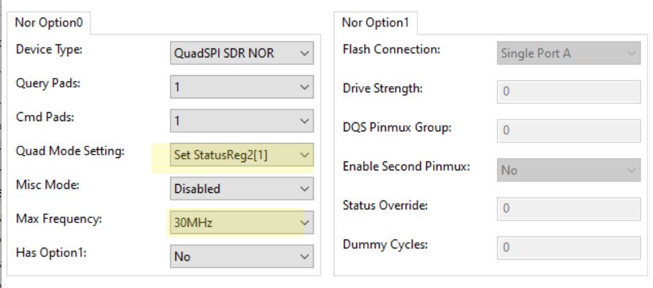
According to the options description, choose:
OPTION 0: 0xc0000201
OPTION 1:0x0
Just like this situation:
Fig 4
3.1 RT-UFL code modification
Here, use the keil project:
\RT-UFL-1.0\build\mdk
The code modification is as follows:
Ufl_main.c: ufl_set_target_property1
 case kChipId_RT105x:
            uflTargetDesc->flexspiInstance = MIMXRT105X_1st_FLEXSPI_INSTANCE;
            uflTargetDesc->flexspiBaseAddr = MIMXRT105X_1st_FLEXSPI_BASE;
            uflTargetDesc->flashBaseAddr   = MIMXRT105X_1st_FLEXSPI_AMBA_BASE;

	//p25q16h QESet bit 1 in Status Register 2  {.option0.U = 0xc0000201, .option1.U = 0x00000000},
            uflTargetDesc->configOption.option0.U = 0xc0000201;
            uflTargetDesc->configOption.option1.U = 0x0;
Ufl_romapi.c: readSampleClkSrc configuration
status_t flexspi_nor_auto_config(uint32_t instance, flexspi_nor_config_t *config, serial_nor_config_option_t *option)
{
    // Wait until the FLEXSPI is idle
    register uint32_t delaycnt = 10000u;
    while(delaycnt--)
    {
    }
    status_t status = flexspi_nor_get_config(instance, config, option);
    if (status != kStatus_Success)
    {
        return status;
    }
config->memConfig.readSampleClksrc=kFlexSPIReadSampleClk_LoopbackInternally; //For DQS is used by other circuit
    return flexspi_nor_flash_init(instance, config);
}
FlashDev.c
struct FlashDevice const FlashDevice = {
   FLASH_DRV_VERS,             // Driver Version, do not modify!
   "MIMXRT_FLEXSPI",           // Device Name
   EXTSPI,                     // Device Type
   0x60000000,                 // Device Start Address
   0x00800000,                 // Device Size in Bytes (8mB)
   256,                        // Programming Page Size
   0,                          // Reserved, must be 0
   0xFF,                       // Initial Content of Erased Memory
   100,                        // Program Page Timeout 100 mSec
   5000,                       // Erase Sector Timeout 5000 mSec

   // Specify Size and Address of Sectors
   0x1000, 0x00000000,         // Sector Size  4kB (256 Sectors)
   SECTOR_END
};
FlashOS.h: it will generate the UFL_L0 type, to define the flash page, sector size
#define FLASH_DRV_SIZE_OPT (0)
#if (FLASH_DRV_SIZE_OPT == 0)
#define FLASH_DRV_PAGE_SIZE      (0x100)
#define FLASH_DRV_SECTOR_SIZE    (0x1000)
#elif (FLASH_DRV_SIZE_OPT == 1)
#define FLASH_DRV_PAGE_SIZE      (0x200)
#define FLASH_DRV_SECTOR_SIZE    (0x1000)
#elif (FLASH_DRV_SIZE_OPT == 2)
#define FLASH_DRV_PAGE_SIZE      (0x200)
#define FLASH_DRV_SECTOR_SIZE    (0x10000)
#endif
Compile the code, it will get flashdriver firmware:MIMXRT_FLEXSPI_UV5_UFL.FLM
Rename it to:MIMXRT_FLEXSPI_UV5_UFL_P25Q16H.FLM
3.2 JLINK driver flashdriver update
After installing the JLINK driver, modify it to use the RT-UFL algorithm.
According to this article, the driving algorithm of JLINK is modified to RT-UFL algorithm:
https://www.cnblogs.com/henjay724/p/14942574.html
In fact, just copy: RT-UFL-1.0\RT-UFL-1.0\algo\SEGGER\JLink_Vxxx
To the installed JLINK path: C:\Program Files\SEGGER\JLINKV768B
But this article need to based on this to add the modified flash algorithm for P25Q16H, the modification points are:
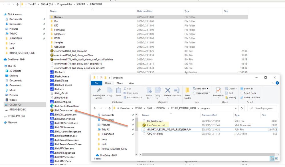
(1)Copy attached file RT1050_P25Q16H_JLINK\program\ JLinkDevices.xml to:
C:\Program Files\SEGGER\JLINKV768B
Fig 5
The .xml modification is as follows, add the P25Q16H item and it’s algorithm:
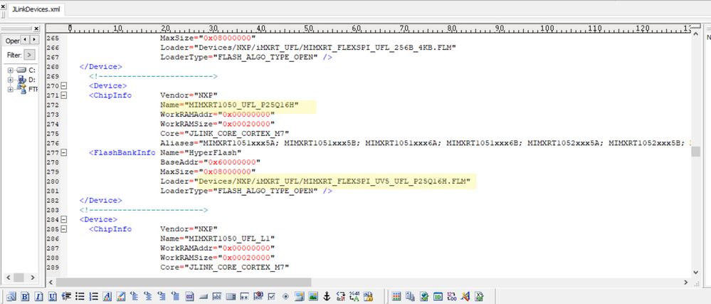
Fig 6
Note: device name is MIMXRT1050_UFL_P25Q16H
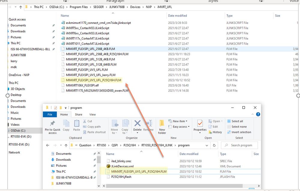
(2) CopyRT1050_P25Q16H_JLINK\program\ IMXRT_FLEXSPI_UV5_UFL_P25Q16H.FLM
to:C:\Program Files\SEGGER\JLINKV768B\Devices\NXP\iMXRT_UFL
Fig 7
This MIMXRT_FLEXSPI_UV5_UFL_P25Q16H.FLM is the modified flashdriver algorithm in the above.
(3)run C:\Program Files\SEGGER\JLINKV768B\JLinkDLLUpdater.exe, update the
modified driver to the IDE IAR
3.3 Flashdriver algorithm downloading test
For MIMXRT1050-EVKB, to use external JLINK, you need to disconnect J33 on the EVKB board and plug JTAG into J21.
3.3.1 Use JFLASH downloading test
First, use the previously modified EVKB-IMXRT1050-flexspi_nor_polling_transfer, disable the QE bit, to simulate the new QSPI flash chip. The test is as follows:
Fig 8
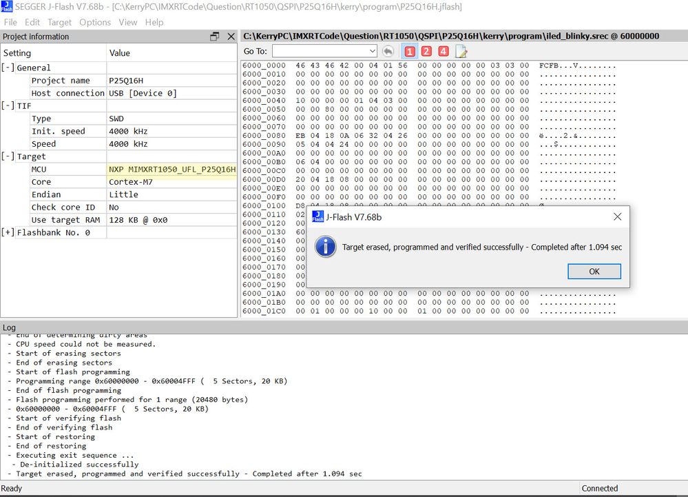
JFlash test result is:
Fig 9
We can see, use the Jflash with new flashdriver, can program the flash successfully.
3.3.2 led_blinky app debug test
Disable the QE bit, to simulate the new QSPI flash chip, the test as Fig 8.
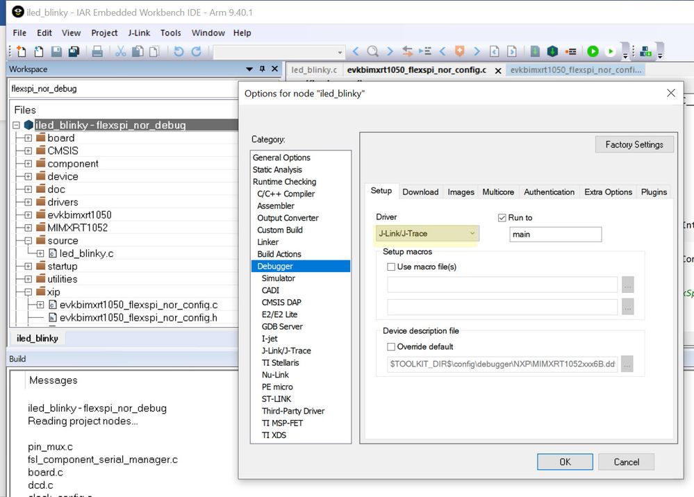
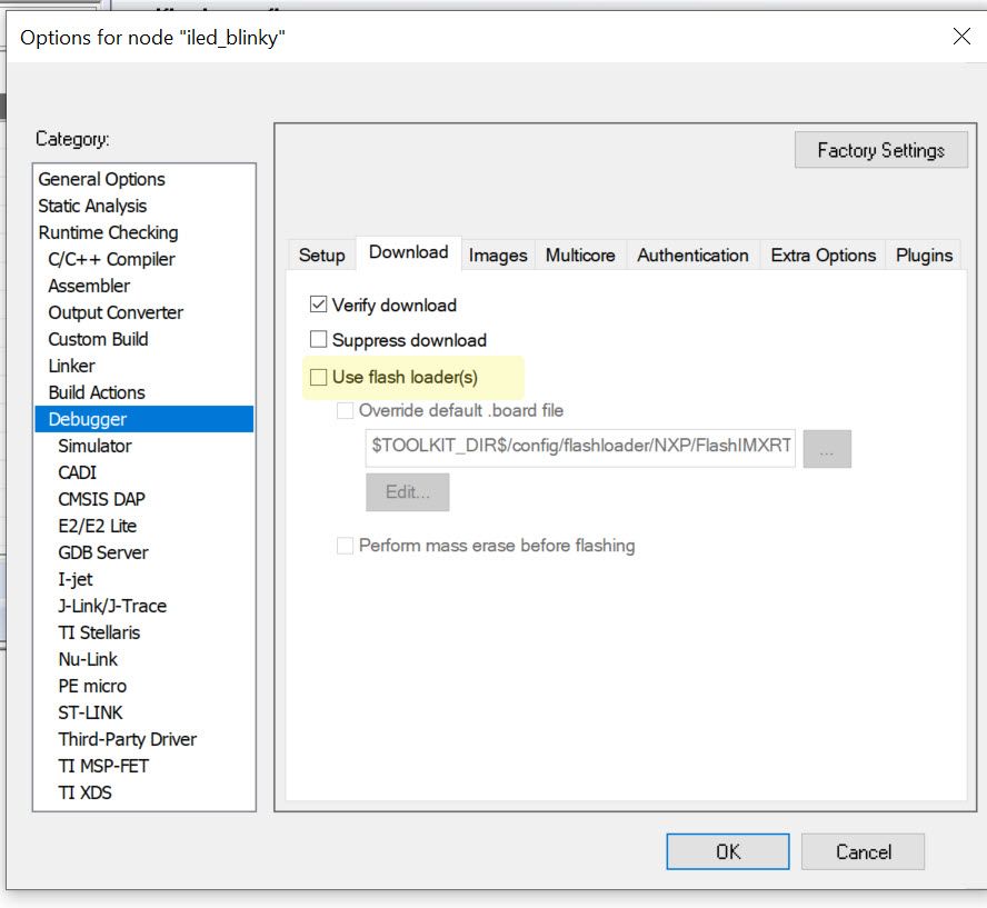
APP demo use the IAR project(customer use it), option select JLINK:
Fig 10
Fig 11
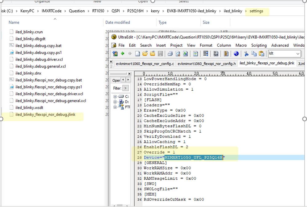
It should be noted here that the device is selected as the modified super download algorithm device name. The method is as follows. The settings->xxx.jlink generated by IAR debug is modified as follows:
Fig 12
Two points: override =1, and device is the new modified algorithm device name.
Debug test result:
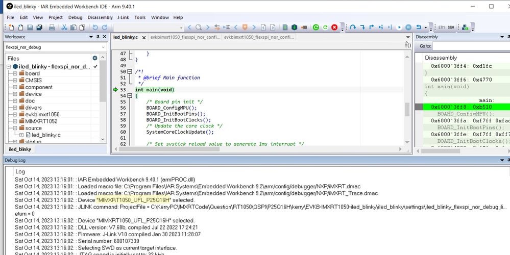
Fig 13
We can see that the algorithm can be successfully debugged and the algorithm is also modified by UFL.
Run it at full speed and you can see the on board LED is flashing.
It means that all flash driver algorithms, hardware, and codes already support the new P25Q16H QSPI flash.
4. Summary
When using a new QSPI flash, first need to pay attention to the position of QE and whether DQS is used, and then prepare the corresponding RT-UFL programming algorithm. The UFL algorithm can usually support most flash chips by default. When QE and DQS are used, they only need to fine-tune the algorithm to support the new QSPI flash. Therefore, this article has successfully solved the problem of burning customer projects after modifying the algorithm. For other QSPI flash, you can also use the method in this article to modify the burning algorithm accordingly to ensure that it meets your own project needs.


