- NXP Forums
- Product Forums
- General Purpose MicrocontrollersGeneral Purpose Microcontrollers
- i.MX Forumsi.MX Forums
- QorIQ Processing PlatformsQorIQ Processing Platforms
- Identification and SecurityIdentification and Security
- Power ManagementPower Management
- MCX Microcontrollers
- S32G
- S32K
- S32V
- MPC5xxx
- Other NXP Products
- Wireless Connectivity
- S12 / MagniV Microcontrollers
- Powertrain and Electrification Analog Drivers
- Sensors
- Vybrid Processors
- Digital Signal Controllers
- 8-bit Microcontrollers
- ColdFire/68K Microcontrollers and Processors
- PowerQUICC Processors
- OSBDM and TBDML
-
- Solution Forums
- Software Forums
- MCUXpresso Software and ToolsMCUXpresso Software and Tools
- CodeWarriorCodeWarrior
- MQX Software SolutionsMQX Software Solutions
- Model-Based Design Toolbox (MBDT)Model-Based Design Toolbox (MBDT)
- FreeMASTER
- eIQ Machine Learning Software
- Embedded Software and Tools Clinic
- S32 SDK
- S32 Design Studio
- GUI Guider
- Zephyr Project
- Voice Technology
- Application Software Packs
- Secure Provisioning SDK (SPSDK)
- Processor Expert Software
-
- Topics
- Mobile Robotics - Drones and RoversMobile Robotics - Drones and Rovers
- NXP Training ContentNXP Training Content
- University ProgramsUniversity Programs
- Rapid IoT
- NXP Designs
- SafeAssure-Community
- OSS Security & Maintenance
- Using Our Community
-
- Cloud Lab Forums
-
- Home
- :
- i.MX Forums
- :
- i.MX RT Knowledge Base
- :
- How to create a new Flash driver of the MCUXPresso IDE
How to create a new Flash driver of the MCUXPresso IDE
- Subscribe to RSS Feed
- Mark as New
- Mark as Read
- Bookmark
- Subscribe
- Printer Friendly Page
- Report Inappropriate Content
How to create a new Flash driver of the MCUXPresso IDE
How to create a new Flash driver of the MCUXPresso IDE
Introduction
Normal Cortex-M core-based MCUs generally have built-in parallel NOR Flash. The parallel NOR Flash is directly hung on the Cortex-M core high-performance AHB bus. If a well-known IDE supports the MCU, it should integrate the corresponding Flash driver algorithm which enables the developer to program and debug the MCU in the IDE.
However, the i.MX RT series MCU doesn't contain the internal flash, how do developers debug these MCUs with online XIP (eXecute-In-Place)?
Take easy, i.MXRT can support external parallel NOR and serial NOR to run the XIP, benefit from saving the number of pins, serial NOR Flash is most commonly used and FlexSPI supports XIP feature which makes online debug available.
The article introduces the mechanism of debugging the external serial NOR flash with the RT MCU and illustrates the steps of modifying the flash driver algorithm of MCUXpresso.
CoreSight Technical
The i.MX RT series MCU is based on the Cortex-M core and the CoreSight Technical is a new debugging architecture launched by ARM in 2004 and is also a part of the core authorization, supports the debug and trace feature for Cortex-M core-based MCU.
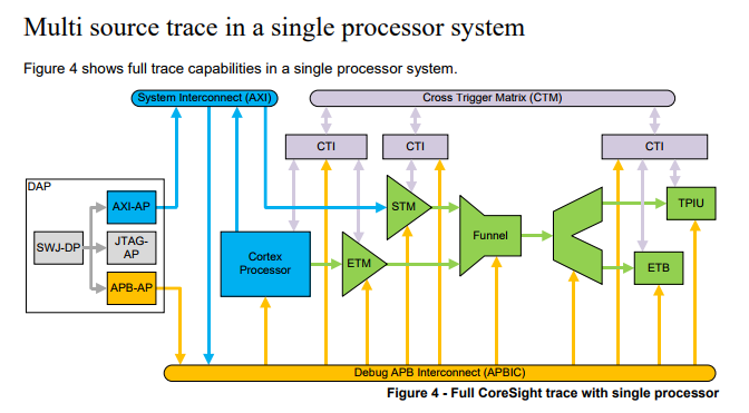
CoreSight is very powerful. It contains many debugging components (ie various protocols). The following figure is from the CoreSight Technical Introduction Manual, which shows the connections between various debugging components under the CoreSight architecture.
This article does not mainly aim to introduce CoreSight technical. Therefore, for CoreSight, we only need to know that it in charge of the main debugging work and the CoreSight can access the system memory and peripheral register from the AMBA bus through the DAP component in real-time, definitely, it includes the code in the external serial Flash.
FlexSPI module
To implement debugging in serial Flash, the code must be XIP in serial Flash, that is, the CPU must be able to fetch instructions and data from any address in serial Flash in real-time. The serial Flash mentioned in this article generally refers to the 4-wire SPI Interface NOR Flash and the SPI mode can be Single/Dual/Quad/Octal.
No matter which SPI mode is, the Flash is essentially serial Flash, and the address lines and data lines are not only shared but also serial. According to conventional knowledge, to implement the XIP, Flash should be a parallel bus interface and hung on AMBA, further, this parallel bus should have independent address lines and data lines, and the width of the address lines correspond to the size of Flash.
So why can run XIP in serial Flash with i.MXRT? The answer is the FlexSPI peripheral.
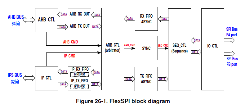
Figure 2 is the FlexSPI module block diagram.
On the right side of the block diagram is the signal connection between FlexSPI and external serial Flash. The left side is the connection between FlexSPI and the internal bus of the i.MXRT system. There are two types of bus interface: 32bit IPS BUS (manual manipulate the FlexSPI register sends Flash reading and writing commands) and 64bit AHB BUS (FlexSPI translates the AHB access address and automatically sends the corresponding Flash reading and writing commands) which is the key feature enables the XIP available.
In the Reference manual, it lists detailed information about the AHB bus:
- AHB RX Buffer implemented to reduce read latency. Total AHB RX Buffer size: 128 * 64 Bits
- 16 AHB masters supported with priority for reading access
- 4 flexible and configurable buffers in AHB RX Buffer
- AHB TX Buffer implemented to buffer all write data from one AHB burst. AHB TX Buffer size: 8 * 64 Bits
- All AHB masters share this AHB TX Buffer. No AHB master number limitation for Write Access.
In addition, the AHB bus includes the below-enhanced features to optimize the reading of Serial Flash memory.
- Cachable and Non-Cachable access
- Prefetch Enable/Disable
- Burst size: 8/16/32/64 bits
- All burst type: SINGLE/INCR/WRAP4/INCR4/WRAP8/INCR8/WRAP16/INCR16
Debugging process of serial Flash
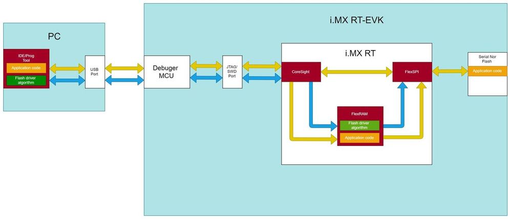
Fig 3 illustrates the debugging process of serial Flash with the RT series MCU and in basic, the overview of the debugging process is not complicated.
When you click IDE debugging icon, the Flash driver algorithm (executable file) pre-installed in the IDE will be downloaded to the internal FlexRAM of i.MXRT via the debugger firstly. The Flash driver algorithm provides FlexSPI initialization, erase and programming APIs, etc.
Next, the debugger caches the application code (binary machine code) in FlexRAM in segments prior to calling the Flash programming API to implement the program work.
After completing programming application code (from FlexRAM to Flash), CoreSight will take over the debugging work.
At this time, the CPU can access the serial Flash that connects the FlexSPI module through the AHB bus, in another word, CoreSight can control and track code in real-time, and single-step debugging is available too in the IDE.
Fig 3
Flash Driver of MCUXpresso IDE
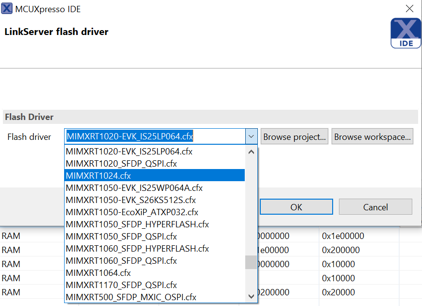
The latest version (11.3.1) of MCUXpresso IDE supports all RT series MCU (as the following figure shows), the developer should select a suitable flash driver file to apply to his board (Fig 5).
Fig 4 MCUXpresso IDE
As mentioned above, the RT series MCUs don't have an internal flash, so they must use an either external parallel or serial NOR.
For IDE providers, it's too hard to provide enough flash drivers to fit all external NOR flashes, the workload is huge, so IDEs general provide the flash driver files for mainstream Serial NOR, especially, 4-wire SPI Interface NOR Flash, it means we need to modify or tune the flash driver to fit our specific application.
Add new flash driver of MCUXpresso IDE
Before start, we should realize that MCUXpresso IDE is different from MDK/IAR. The flash driver algorithms of MDK and IAR are independent of the specific debug tools and they are able to use with all supported debug tools (JLink/DAPLink, etc).
For MCUXpresso IDE, the flash driver algorithms are only able to use with the CMSIS-DAP type debug tool. For instance, when you use JLink with MCUXPresso IDE, it will use the flash driver algorithm of Jlink instead of its own.
There's a real case from a customer:
He currently designs his new card reader module based on RT1024 and he plans to make a board without external RAM and Flash.
In other words, he only utilizes the internal 4MB flash and 256KB FlexRAM which consist of SRAM_DTC(64KB), SRAM_ITC(64KB), SRAM_OC(128KB).
So he wants to configure the 256KB RAM area as normal 256KB RAM without being allocated to ITCM and DTCM.
He follows the thread to reconfigure the FlexRAM, but he still encounters the below problem (as Fig 6 shows ) when entering debug mode.
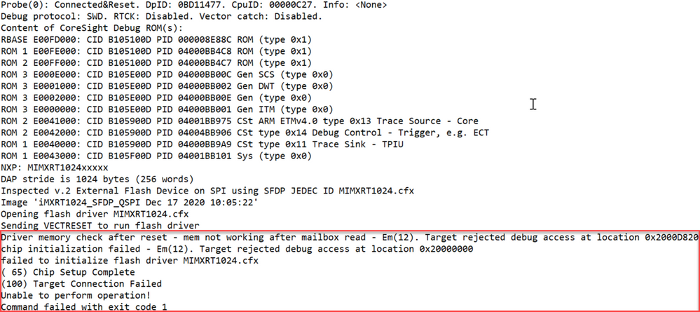
According to the debug failure log, we can come to a conclusion that the flash drive file: MIMXRT1020.cfx needs to be updated, and the following steps illustrate how to do it.
a) Select a source project
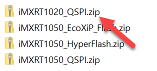
There are some flash driver projects in the Examples/Flashdrivers/NXP subdirectory within the MCUXpresso IDE installation directory (as Fig 7 shows) and iMXRT folder contains some flash driver projects for external flash parts that work with the RT series MCU (as Fig 8 shows).
Fig 7
Fig 8
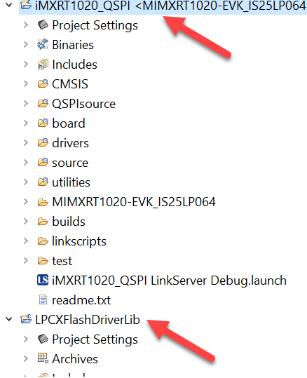
Select the flash driver project which is the closest to the target as a prototype, in this case, we select the iMXRT1020_QSPI project, extract the project file and import them in the MCUXpresso IDE (as Fig 9).
Fig 9
b) Modify pin assignment
The RT1024 integrates a 4 MB QSPI flash as an "internal flash", it is connected to different FlexSPI pins versus to the default pins of the iMXRT1020_QSPI project just as the below table shows.
| FlexSPI pin | RT1020 | RT1024 |
|---|---|---|
| FLEXSPI_A_DQS | GPIO_SD_B1_05 | GPIO_SD_B1_05 |
| FLEXSPI_A_SS0_B | GPIO_SD_B1_11 | GPIO_AD_B1_05 |
| FLEXSPI_A_SCLK | GPIO_SD_B1_07 | GPIO_AD_B1_01 |
| FLEXSPI_A_DATA0 | GPIO_SD_B1_08 | GPIO_AD_B1_02 |
| FLEXSPI_A_DATA1 | GPIO_SD_B1_10 | GPIO_AD_B1_04 |
| FLEXSPI_A_DATA2 | GPIO_SD_B1_09 | GPIO_AD_B1_03 |
| FLEXSPI_A_DATA3 | GPIO_SD_B1_06 | GPIO_AD_B1_00 |
So it needs to adjust the pin initialization in the BOARD_InitPins() function in pin_mux.c.
/* FUNCTION ************************************************************************************************************
 *
 * Function Name : BOARD_InitPins
 * Description   : Configures pin routing and optionally pin electrical features.
 *
 * END ****************************************************************************************************************/
void BOARD_InitPins(void) {
  CLOCK_EnableClock(kCLOCK_Iomuxc);           /* iomuxc clock (iomuxc_clk_enable): 0x03u */

  IOMUXC_SetPinMux(
      IOMUXC_GPIO_AD_B0_06_LPUART1_TX,        /* GPIO_AD_B0_06 is configured as LPUART1_TX */
      0U);                                    /* Software Input On Field: Input Path is determined by functionality */
  IOMUXC_SetPinMux(
      IOMUXC_GPIO_AD_B0_07_LPUART1_RX,        /* GPIO_AD_B0_07 is configured as LPUART1_RX */
      0U);                                    /* Software Input On Field: Input Path is determined by functionality */
  IOMUXC_SetPinMux(
      IOMUXC_GPIO_SD_B1_05_FLEXSPI_A_DQS,     /* GPIO_SD_B1_05 is configured as FLEXSPI_A_DQS */
      1U);                                    /* Software Input On Field: Force input path of pad GPIO_SD_B1_05 */
//  IOMUXC_SetPinMux(
//      IOMUXC_GPIO_SD_B1_06_FLEXSPI_A_DATA03,  /* GPIO_SD_B1_06 is configured as FLEXSPI_A_DATA03 */
//      1U);                                    /* Software Input On Field: Force input path of pad GPIO_SD_B1_06 */
//  IOMUXC_SetPinMux(
//      IOMUXC_GPIO_SD_B1_07_FLEXSPI_A_SCLK,    /* GPIO_SD_B1_07 is configured as FLEXSPI_A_SCLK */
//      1U);                                    /* Software Input On Field: Force input path of pad GPIO_SD_B1_07 */
//  IOMUXC_SetPinMux(
//      IOMUXC_GPIO_SD_B1_08_FLEXSPI_A_DATA00,  /* GPIO_SD_B1_08 is configured as FLEXSPI_A_DATA00 */
//      1U);                                    /* Software Input On Field: Force input path of pad GPIO_SD_B1_08 */
//  IOMUXC_SetPinMux(
//      IOMUXC_GPIO_SD_B1_09_FLEXSPI_A_DATA02,  /* GPIO_SD_B1_09 is configured as FLEXSPI_A_DATA02 */
//      1U);                                    /* Software Input On Field: Force input path of pad GPIO_SD_B1_09 */
//  IOMUXC_SetPinMux(
//      IOMUXC_GPIO_SD_B1_10_FLEXSPI_A_DATA01,  /* GPIO_SD_B1_10 is configured as FLEXSPI_A_DATA01 */
//      1U);                                    /* Software Input On Field: Force input path of pad GPIO_SD_B1_10 */
//  IOMUXC_SetPinMux(
//      IOMUXC_GPIO_SD_B1_11_FLEXSPI_A_SS0_B,   /* GPIO_SD_B1_11 is configured as FLEXSPI_A_SS0_B */
//      1U);                                    /* Software Input On Field: Force input path of pad GPIO_SD_B1_11 */

  IOMUXC_SetPinMux(
      IOMUXC_GPIO_AD_B1_00_FLEXSPI_A_DATA03,  /* GPIO_AD_B1_00 is configured as FLEXSPI_A_DATA03 */
      1U);                                    /* Software Input On Field: Force input path of pad GPIO_AD_B1_00 */
  IOMUXC_SetPinMux(
     IOMUXC_GPIO_AD_B1_01_FLEXSPI_A_SCLK,    /* GPIO_AD_B1_01 is configured as FLEXSPI_A_SCLK */
      1U);                                    /* Software Input On Field: Force input path of pad GPIO_AD_B1_01 */
  IOMUXC_SetPinMux(
     IOMUXC_GPIO_AD_B1_02_FLEXSPI_A_DATA00,  /* GPIO_AD_B1_02 is configured as FLEXSPI_A_DATA00 */
      1U);                                    /* Software Input On Field: Force input path of pad GPIO_AD_B1_02 */
  IOMUXC_SetPinMux(
     IOMUXC_GPIO_AD_B1_03_FLEXSPI_A_DATA02,  /* GPIO_AD_B1_03 is configured as FLEXSPI_A_DATA02 */
      1U);                                    /* Software Input On Field: Force input path of pad GPIO_AD_B1_03 */
  IOMUXC_SetPinMux(
     IOMUXC_GPIO_AD_B1_04_FLEXSPI_A_DATA01,  /* GPIO_AD_B1_04 is configured as FLEXSPI_A_DATA01 */
      1U);                                    /* Software Input On Field: Force input path of pad GPIO_AD_B1_04 */
  IOMUXC_SetPinMux(
     IOMUXC_GPIO_AD_B1_05_FLEXSPI_A_SS0_B,   /* GPIO_AD_B1_05 is configured as FLEXSPI_A_SS0_B */
      1U);                                    /* Software Input On Field: Force input path of pad GPIO_AD_B1_05 */
  IOMUXC_SetPinConfig(
      IOMUXC_GPIO_AD_B0_06_LPUART1_TX,        /* GPIO_AD_B0_06 PAD functional properties : */
      0x10B0u);                               /* Slew Rate Field: Slow Slew Rate
                                                 Drive Strength Field: R0/6
                                                 Speed Field: medium(100MHz)
                                                 Open Drain Enable Field: Open Drain Disabled
                                                 Pull / Keep Enable Field: Pull/Keeper Enabled
                                                 Pull / Keep Select Field: Keeper
                                                 Pull Up / Down Config. Field: 100K Ohm Pull Down
                                                 Hyst. Enable Field: Hysteresis Disabled */
  IOMUXC_SetPinConfig(
      IOMUXC_GPIO_AD_B0_07_LPUART1_RX,        /* GPIO_AD_B0_07 PAD functional properties : */
      0x10B0u);                               /* Slew Rate Field: Slow Slew Rate
                                                 Drive Strength Field: R0/6
                                                 Speed Field: medium(100MHz)
                                                 Open Drain Enable Field: Open Drain Disabled
                                                 Pull / Keep Enable Field: Pull/Keeper Enabled
                                                 Pull / Keep Select Field: Keeper
                                                 Pull Up / Down Config. Field: 100K Ohm Pull Down
                                                 Hyst. Enable Field: Hysteresis Disabled */
  IOMUXC_SetPinConfig(
      IOMUXC_GPIO_SD_B1_05_FLEXSPI_A_DQS,     /* GPIO_SD_B1_05 PAD functional properties : */
      0x10F1u);                               /* Slew Rate Field: Fast Slew Rate
                                                 Drive Strength Field: R0/6
                                                 Speed Field: max(200MHz)
                                                 Open Drain Enable Field: Open Drain Disabled
                                                 Pull / Keep Enable Field: Pull/Keeper Enabled
                                                 Pull / Keep Select Field: Keeper
                                                 Pull Up / Down Config. Field: 100K Ohm Pull Down
                                                 Hyst. Enable Field: Hysteresis Disabled */
  IOMUXC_SetPinConfig(
      IOMUXC_GPIO_SD_B1_06_FLEXSPI_A_DATA03,  /* GPIO_SD_B1_06 PAD functional properties : */
      0x10F1u);                               /* Slew Rate Field: Fast Slew Rate
                                                 Drive Strength Field: R0/6
                                                 Speed Field: max(200MHz)
                                                 Open Drain Enable Field: Open Drain Disabled
                                                 Pull / Keep Enable Field: Pull/Keeper Enabled
                                                 Pull / Keep Select Field: Keeper
                                                 Pull Up / Down Config. Field: 100K Ohm Pull Down
                                                 Hyst. Enable Field: Hysteresis Disabled */
  IOMUXC_SetPinConfig(
      IOMUXC_GPIO_SD_B1_07_FLEXSPI_A_SCLK,    /* GPIO_SD_B1_07 PAD functional properties : */
      0x10F1u);                               /* Slew Rate Field: Fast Slew Rate
                                                 Drive Strength Field: R0/6
                                                 Speed Field: max(200MHz)
                                                 Open Drain Enable Field: Open Drain Disabled
                                                 Pull / Keep Enable Field: Pull/Keeper Enabled
                                                 Pull / Keep Select Field: Keeper
                                                 Pull Up / Down Config. Field: 100K Ohm Pull Down
                                                 Hyst. Enable Field: Hysteresis Disabled */
  IOMUXC_SetPinConfig(
      IOMUXC_GPIO_SD_B1_08_FLEXSPI_A_DATA00,  /* GPIO_SD_B1_08 PAD functional properties : */
      0x10F1u);                               /* Slew Rate Field: Fast Slew Rate
                                                 Drive Strength Field: R0/6
                                                 Speed Field: max(200MHz)
                                                 Open Drain Enable Field: Open Drain Disabled
                                                 Pull / Keep Enable Field: Pull/Keeper Enabled
                                                 Pull / Keep Select Field: Keeper
                                                 Pull Up / Down Config. Field: 100K Ohm Pull Down
                                                 Hyst. Enable Field: Hysteresis Disabled */
  IOMUXC_SetPinConfig(
      IOMUXC_GPIO_SD_B1_09_FLEXSPI_A_DATA02,  /* GPIO_SD_B1_09 PAD functional properties : */
      0x10F1u);                               /* Slew Rate Field: Fast Slew Rate
                                                 Drive Strength Field: R0/6
                                                 Speed Field: max(200MHz)
                                                 Open Drain Enable Field: Open Drain Disabled
                                                 Pull / Keep Enable Field: Pull/Keeper Enabled
                                                 Pull / Keep Select Field: Keeper
                                                 Pull Up / Down Config. Field: 100K Ohm Pull Down
                                                 Hyst. Enable Field: Hysteresis Disabled */
  IOMUXC_SetPinConfig(
      IOMUXC_GPIO_SD_B1_10_FLEXSPI_A_DATA01,  /* GPIO_SD_B1_10 PAD functional properties : */
      0x10F1u);                               /* Slew Rate Field: Fast Slew Rate
                                                 Drive Strength Field: R0/6
                                                 Speed Field: max(200MHz)
                                                 Open Drain Enable Field: Open Drain Disabled
                                                 Pull / Keep Enable Field: Pull/Keeper Enabled
                                                 Pull / Keep Select Field: Keeper
                                                 Pull Up / Down Config. Field: 100K Ohm Pull Down
                                                 Hyst. Enable Field: Hysteresis Disabled */
  IOMUXC_SetPinConfig(
      IOMUXC_GPIO_SD_B1_11_FLEXSPI_A_SS0_B,   /* GPIO_SD_B1_11 PAD functional properties : */
      0x10F1u);                               /* Slew Rate Field: Fast Slew Rate
                                                 Drive Strength Field: R0/6
                                                 Speed Field: max(200MHz)
                                                 Open Drain Enable Field: Open Drain Disabled
                                                 Pull / Keep Enable Field: Pull/Keeper Enabled
                                                 Pull / Keep Select Field: Keeper
                                                 Pull Up / Down Config. Field: 100K Ohm Pull Down
                                                 Hyst. Enable Field: Hysteresis Disabled */
}
c) Modify linker file
According to Fig 3, a flash driver should be downloaded into FlexRAM on the target MCU during the debuggingprocess, for the iMXRT1020_QSPI project, the flash driver needs to be downloaded to DTCM (0x2000_0000~0x2001_0000), however, to meet the customer's demand, the whole of FlexRAM is reconfigured to SRAM_OC in the ResetISR() function. In another word,
there's no DTCM area to load the flash driver and it causes the above debug failure.
So we need to use the SRAM_OC instead of DTCM to load the flash driver just like the below shows.
In the FlashDriver_32Kbuffer.ld of iMXRT1020_QSPI project:
/*
 * Linker script for NXP LPC546xx SPIFI Flash Driver (Messaged)
*/

MEMORY
{
      /*SRAM (rwx) : ORIGIN = 0x20000000, LENGTH = (64 * 1024)*/
      SRAM (rwx) : ORIGIN = 0x20200000, LENGTH = (64 * 1024)
}

/* stack size :  multiple of 8*/
__stack_size = (4 * 1024);

/* flash image buffer size : multiple of page size*/
__cache_size = (32 * 1024);

/* Supported operations bit map
 * 0x40 = New device info available after Init() call
 * This setting must match the actual target flash driver build!
 */
 __opmap_val = 0x1000;

/* Actual placement of flash driver code/data controlled via standard file */
INCLUDE "../../LPCXFlashDriverLib/linker/placement.ld"
d) Recompile
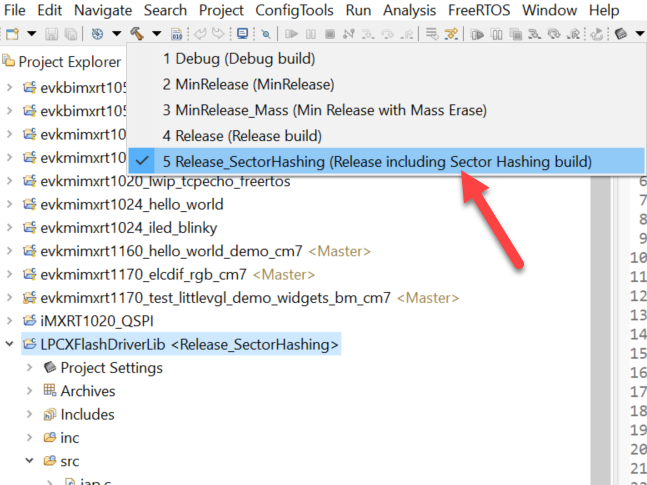
In the LPCXFlashDriverLib project, select the Release_SectorHashing option prior to clicking the Build icon to generate libLPCXFlashDriverLib.a file (as Fig 10 shows).
Fig 10
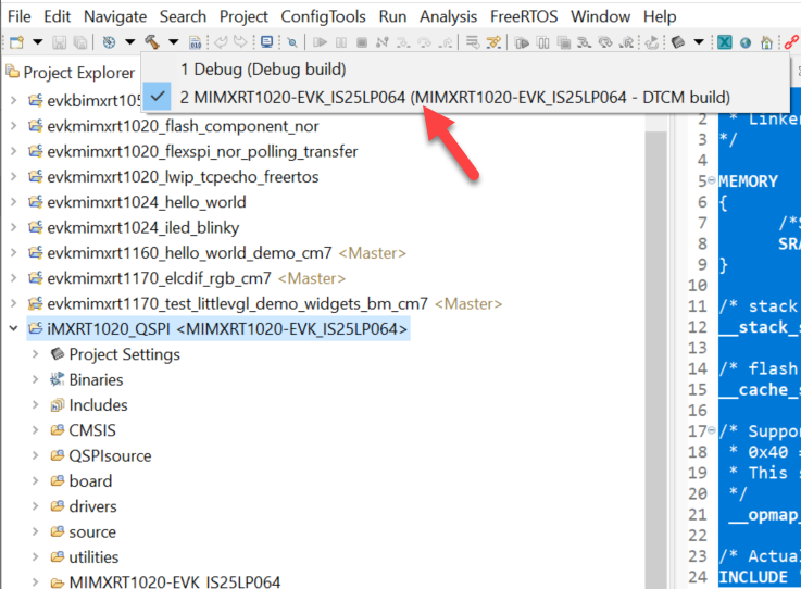
Next, in the iMXRT1020_QSPI project, select the MIMXRT1020-EVK_IS25LP064 option (as Fig 11 shows), then click the Build icon to generate a new flash driver file that resides in ~\Examples\Flashdrivers\NXP\iMXRT\iMXRT1020_QSPI\iMXRT1020_QSPI\builds directory.
Fig 11
Note: I've attached a test project which is based on the hello_world demo that comes from the RT1024's SDK library, in addition, the attachment also contains the new flash driver and corresponding debug script files, so please give it a try.
