- Forums
- Product Forums
- General Purpose MicrocontrollersGeneral Purpose Microcontrollers
- i.MX Forumsi.MX Forums
- QorIQ Processing PlatformsQorIQ Processing Platforms
- Identification and SecurityIdentification and Security
- Power ManagementPower Management
- Wireless ConnectivityWireless Connectivity
- RFID / NFCRFID / NFC
- Advanced AnalogAdvanced Analog
- MCX Microcontrollers
- S32G
- S32K
- S32V
- MPC5xxx
- Other NXP Products
- S12 / MagniV Microcontrollers
- Powertrain and Electrification Analog Drivers
- Sensors
- Vybrid Processors
- Digital Signal Controllers
- 8-bit Microcontrollers
- ColdFire/68K Microcontrollers and Processors
- PowerQUICC Processors
- OSBDM and TBDML
- S32M
- S32Z/E
-
- Solution Forums
- Software Forums
- MCUXpresso Software and ToolsMCUXpresso Software and Tools
- CodeWarriorCodeWarrior
- MQX Software SolutionsMQX Software Solutions
- Model-Based Design Toolbox (MBDT)Model-Based Design Toolbox (MBDT)
- FreeMASTER
- eIQ Machine Learning Software
- Embedded Software and Tools Clinic
- S32 SDK
- S32 Design Studio
- GUI Guider
- Zephyr Project
- Voice Technology
- Application Software Packs
- Secure Provisioning SDK (SPSDK)
- Processor Expert Software
- Generative AI & LLMs
-
- Topics
- Mobile Robotics - Drones and RoversMobile Robotics - Drones and Rovers
- NXP Training ContentNXP Training Content
- University ProgramsUniversity Programs
- Rapid IoT
- NXP Designs
- SafeAssure-Community
- OSS Security & Maintenance
- Using Our Community
-
- Cloud Lab Forums
-
- Knowledge Bases
- ARM Microcontrollers
- i.MX Processors
- Identification and Security
- Model-Based Design Toolbox (MBDT)
- QorIQ Processing Platforms
- S32 Automotive Processing Platform
- Wireless Connectivity
- CodeWarrior
- MCUXpresso Suite of Software and Tools
- MQX Software Solutions
- RFID / NFC
- Advanced Analog
-
- NXP Tech Blogs
- Home
- :
- i.MXプロセッサ
- :
- i.MX RT Crossover MCUs Knowledge Base
- :
- How to configure SRAM in SEMC modules for RT devices
How to configure SRAM in SEMC modules for RT devices
- RSS フィードを購読する
- 新着としてマーク
- 既読としてマーク
- ブックマーク
- 購読
- 印刷用ページ
- 不適切なコンテンツを報告
How to configure SRAM in SEMC modules for RT devices
How to configure SRAM in SEMC modules for RT devices
This article will help you understand in detail the necessary steps to connect an external SRAM memory to the RT devices with the SEMC module. This document is focused on RT1170 however a lot of this information can also be followed for other RT devices with the SEMC module, please consult limitations on the specific device Reference Manual.
In this post, there is attached an example of this, since the EVK does not contain an SRAM a specific memory is not used for this. This is a theoretical approach to how to set this kind of memory.
The user needs to set specific parameters for the memory to be used.
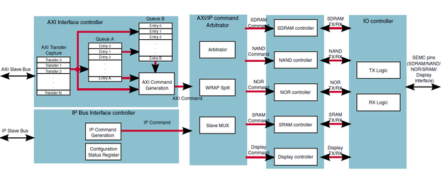
The SEMC is a multi-standard memory controller optimized for both high performance and low pin count. It can support multiple external memories in the same application with shared address and data pins. The interface supported includes SDRAM, NOR Flash, SRAM, and NAND Flash, as well as the 8080 display interface.
Features
The SEMC includes the following features:
- SRAM interface
- Supports SRAM and Pseudo SRAM
- Supports 8/16 bit modes
- Supports ADMUX, AADM, and Non-ADMUX modes
- Up to 4 Chip Select (CS)
- Up to 4096Mb memory size
NOTE
- For 16-bit devices, up to 4096Mb memory size
- For 8-bit devices, up to 2048Mb memory size
For more detailed features on supported memories of this module please consult Reference Manual
How to set SRAM
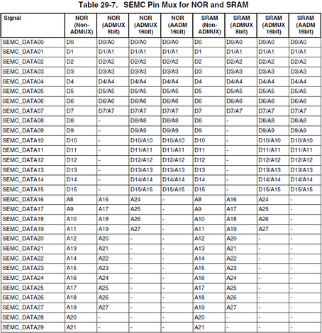
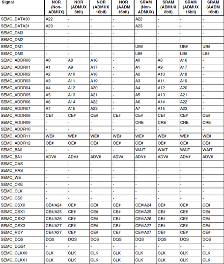
It is important to mention that RT1170 supports ASYNC and SYNC mode on the SRAM however SYNC mode is not supported in all RT devices, e.g. RT1050 does not support SRAM SYNC mode. It is important to consider the pin mux for these devices, for this you can refer to table 29-7 for the RT1170.
Please consider that pins controlled through the IOCR register should be static. This means that if you configure, for example, SEMC_ADDR08 to be CE on the SRAM it cannot be used in the same application as A8 in an SDRAM.
Let´s go step by step on how to configure the parameters and where to find that information:
- Configure MCR[DQSMD] bit to select the read clock source for synchronous mode. Suggest setting it with 0x1 to reach high clock frequency.
config.dqsMode = kSEMC_Loopbackdqspad;- Configure the IOCR register to choose CS pins. For this, you can refer to table 29-6. I suggest using CSX pins for CS signals of the SRAM. The Init function from the SDK sets this register incorrectly so write this register outside the function
SEMC->IOCR |= 0x00908BB6; // A8:CE#0, CSX0:A24, CSX1:A25, CSX2:CE#1, RDY:CE#2- Optional Configure BMCR registers for bus access efficiency, the arbitration adopts a weight-based algorithm where the weights are obtained from BMCR registers. A score is calculated and the command with the highest score is served first. The score is calculated with the following formula:
SCORE = QOS*WQOS + AGE*WAGE/4 + WSH + WRWS
Where :
- QOS stands for AxQOS of AXI bus-WQOS is the weight factor of QOS.
-AGE stands for the wait period for each command
-WAGE is the weight factor of AGE.
-WSH stands for the weight of slave hit without read/write switch scenario.
-WRWS stands for the weight of the slave hit with read/write switch scenario.
This is used when you have multiple devices connected to the module and you want to assign access priorities to the different devices.
- Configure Base Register 6/9/10/11 with base address, memory size, and valid information.
BRx[BA]: In this field, you set the address where the SRAM is going to be located. You can refer to the specific device memory map. In the example, I used 0x9000_0000 but you can use any SEMC location as long it does not overlap with other memory spaces.
BRx[MS]: Here you specify the size of the SRAM. [Image from register]
BRx[VLD] must be 1 so the memory can be accessed.
//VLD is always set to 1 in the SRAM Init function of the SDK
sram_config.address = SRAM_BASE;// Base address 0x90000000 (BR6[BA])
sram_config.memsize_kbytes = 0x10000;// SRAM0 space size 64MB (BR6[MS])
- Configure INTEN and INTR registers if need to generate interrupts. You can use the function "SEMC_EnableInterrupts()"
- Configure SRAM Control Register with parameters obtained from the specific SRAM device. These registers contain the timings for the memory used. These values are obtained from the memory datasheet.
These values are for reference and do not suggest the exact values for a specific SRAM.sram_config.addrPortWidth = 8;// Port width (SRAMCR0[COL])Don't care in SRAM. sram_config.advActivePolarity = kSEMC_AdvActiveLow;//ADV# polarity //(SRAMCR0[ADVP])Don't care if not use ADV. sram_config.addrMode = kSEMC_AddrDataNonMux;//Non Mux mode(SRAMCR0[AM]) sram_config.burstLen = kSEMC_Nor_BurstLen1;//Burst length (SRAMCR0[BL]) sram_config.portSize = kSEMC_PortSize16Bit;//Port size 16bit (SRAMCR0[PS]) sram_config.syncMode = kSEMC_AsyncMode;// ASYNC mode (SRAMCR0[SYNCEN]) sram_config.waitEnable = true;// WAIT enable (SRAMCR0[WAITEN]) sram_config.waitSample = 0;// WAIT sample (SRAMCR0[WAITSP]) sram_config.advLevelCtrl = kSEMC_AdvHigh;// ADV# level control(SRAMCR0[ADVH]) //Don't care if not use ADV. sram_config.tCeSetup_Ns = 20;//CE#setup time[nsec](SRAMCR1[CES])Need tuning. sram_config.tCeHold_Ns = 20;// CE#hold time [nsec](SRAMCR1[CEH]) Need tuning. sram_config.tCeInterval_Ns = 20;//CE#interval time[nsec](SRAMCR2[CEITV]) Need //tuning. sram_config.readHoldTime_Ns = 20;//Read hold time[nsec](SRAMCR2[RDH])Only for //SYNC mode. sram_config.tAddrSetup_N s= 20;//ADDRsetup time[nsec](SRAMCR1[AS])Need tuning. sram_config.tAddrHold_Ns = 20;//ADDRhold time[nsec](SRAMCR1[AH]) Need tuning. sram_config.tWeLow_Ns = 20;//WE low time [nsec] (SRAMCR1[WEL]) Need tuning. sram_config.tWeHigh_Ns = 20;//WE high time [nsec] (SRAMCR1[WEH]) Need tuning. sram_config.tReLow_Ns = 20;// RE low time [nsec] (SRAMCR1[REL]) Need tuning. sram_config.tReHigh_Ns = 20;// RE high time[nsec](SRAMCR1[REH]) Need tuning. sram_config.tTurnAround_Ns = 20;//Turnaround time[nsec](SRAMCR2[TA])Need //tuning but don't set it to be 0. sram_config.tAddr2WriteHold_Ns = 20;//Address to write data hold time [nsec] (SRAMCR2[AWDH]) Need tuning. sram_config.tWriteSetup_Ns = 20;//Write Data setup time[nsec](SRAMCR2[WDS]) //Only for SYNC mode. sram_config.tWriteHold_Ns= 20;//Write Data hold time [nsec] (SRAMCR2[WDH]) //Only for SYNC mode. sram_config.latencyCount = 20;//Latency count[nsec](SRAMCR2[LC]) Only for //SYNC mode. sram_config.readCycle = 20;// read time[nsec](SRAMCR2[RD])Only for SYNC mode. sram_config.delayChain = 20;// typically not used in SRAM. (DCCR [SRAMXVAL], //DCCR [SRAMXEN], DCCR [SRAM0VAL], DCCR [SRAM0EN]) - Initialize the SRAM device by IP command registers (IPCR0/1/2, IPCMD, and IPTXDAT) if needed.
Notes:
-Configure independent timing for SRAM device 0 and device 1/2/3
-Configure SRAM device 0 timing with register SRAMCR0~SRAMCR3
-Configure SRAM decive1/2/3 timing with register SRAMCR4~SRAMCR6


