- Forums
- Product Forums
- General Purpose MicrocontrollersGeneral Purpose Microcontrollers
- i.MX Forumsi.MX Forums
- QorIQ Processing PlatformsQorIQ Processing Platforms
- Identification and SecurityIdentification and Security
- Power ManagementPower Management
- Wireless ConnectivityWireless Connectivity
- RFID / NFCRFID / NFC
- MCX Microcontrollers
- S32G
- S32K
- S32V
- MPC5xxx
- Other NXP Products
- S12 / MagniV Microcontrollers
- Powertrain and Electrification Analog Drivers
- Sensors
- Vybrid Processors
- Digital Signal Controllers
- 8-bit Microcontrollers
- ColdFire/68K Microcontrollers and Processors
- PowerQUICC Processors
- OSBDM and TBDML
- S32M
-
- Solution Forums
- Software Forums
- MCUXpresso Software and ToolsMCUXpresso Software and Tools
- CodeWarriorCodeWarrior
- MQX Software SolutionsMQX Software Solutions
- Model-Based Design Toolbox (MBDT)Model-Based Design Toolbox (MBDT)
- FreeMASTER
- eIQ Machine Learning Software
- Embedded Software and Tools Clinic
- S32 SDK
- S32 Design Studio
- GUI Guider
- Zephyr Project
- Voice Technology
- Application Software Packs
- Secure Provisioning SDK (SPSDK)
- Processor Expert Software
-
- Topics
- Mobile Robotics - Drones and RoversMobile Robotics - Drones and Rovers
- NXP Training ContentNXP Training Content
- University ProgramsUniversity Programs
- Rapid IoT
- NXP Designs
- SafeAssure-Community
- OSS Security & Maintenance
- Using Our Community
-
- Cloud Lab Forums
-
- Knowledge Bases
- ARM Microcontrollers
- i.MX Processors
- Identification and Security
- Model-Based Design Toolbox (MBDT)
- QorIQ Processing Platforms
- S32 Automotive Processing Platform
- Wireless Connectivity
- CodeWarrior
- MCUXpresso Suite of Software and Tools
- MQX Software Solutions
- RFID / NFC
-
- Home
- :
- i.MX论坛
- :
- i.MX RT 交叉 MCU
- :
- Re: target crashes writing to register SW_MUX_CTL_PAD_GPIO_SD_B1_05
target crashes writing to register SW_MUX_CTL_PAD_GPIO_SD_B1_05
target crashes writing to register SW_MUX_CTL_PAD_GPIO_SD_B1_05
Hi,
I have an issue configuring an IOMUX control register for GPIO configuration.
The register in question is SW_MUX_CTL_PAD_GPIO_SD_B1_05, when I write to it using the SDK function IOMUXC_SetPinMux() the target/debugger crashes. This is to configure pin GPIO_SD_B1_04 for use as GPIO.
code:
// GPIO_SD_B1_04
IOMUXC_SetPinMux(IOMUXC_GPIO_SD_B1_04_GPIO3_IO04, 0U);
If I comment out the above line, my code runs fine.
I have lots of other identical calls to this function for configuring other pins for GPIO (100+ of them) and they all work fine.
I checked the address in the .h header file and it looks OK to me.
Any ideas what might be causing this please?
thanks
Nick
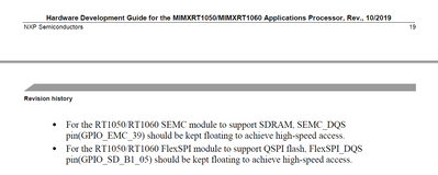
Also see this note from the hardware development guide
-Nick
Hi @nxf48158 , do you have any update on this issue please and the solution proposed by @mjbcswitzerland
thanks and regards
-Nick
Hello Nick,
Hope you are doing well.
Could you please provide the version of the SDK and the IDE you are using so that I may replicate it from my end.
Best Regards,
Sabina
-----------------------------------------------------------------------------------------------------------------------
Note: If this post answers your question, please click the Correct Answer button. Thank you!
-----------------------------------------------------------------------------------------------------------------------
Hi Sabina,
Thank you for your message.
IDE is MCUXpresso IDE v11.1.1 [Build 3241] [2020-03-02] and SDK is 2.7.0
thanks
-Nick
Hi Mark,
It's pad GPIO_SD_B1_05
I notice on the NXP 1062 dev board, this pad is used for FlexSPI_DQS. But my project is configured for standard QSPI flash, not octal hyperflash. And I can program/erase the QSPI flash just fine, and the board boots quite happily from the QSPI after a power cycle - so long as I don't write to that register that is.
I tried 3 different MUX settings for configuring that pad - as GPIO, as FlexSPI_DQS or as FLEXSPI_B_SS0_B. It doesn't seem to make any difference, it crashes with any of those settings.
I'll try your other suggestions, but at the moment I am struggling to get mcuxpresso to display the iomuxc registers for some reason
Thanks again for your help,
regards Nick
Hi Nick
Which PAD is it:
GPIO_SD_B1_04 or GPIO_SD_B1_05?
These are the defines that I have for them:
#define GPIO_SD_B1_04_USDHC2_CLK (IOMUXC_SW_MUX_CTL_PAD_MUX_MODE_ALT0)
#define GPIO_SD_B1_04_FLEXSPI_B_SCLK (IOMUXC_SW_MUX_CTL_PAD_MUX_MODE_ALT1)
#define GPIO_SD_B1_04_LPI2C1_SCL (IOMUXC_SW_MUX_CTL_PAD_MUX_MODE_ALT2)
#define GPIO_SD_B1_04_SAI1_RX_SYNC (IOMUXC_SW_MUX_CTL_PAD_MUX_MODE_ALT3)
#define GPIO_SD_B1_04_FLEXSPIA_SS1_B (IOMUXC_SW_MUX_CTL_PAD_MUX_MODE_ALT4)
#define GPIO_SD_B1_04_GPIO3_IO04 (IOMUXC_SW_MUX_CTL_PAD_MUX_MODE_ALT5)
#define GPIO_SD_B1_04_CCM_STOP (IOMUXC_SW_MUX_CTL_PAD_MUX_MODE_ALT6)
#define GPIO_SD_B1_04_SAI3_MCLK (IOMUXC_SW_MUX_CTL_PAD_MUX_MODE_ALT8)
#define GPIO_SD_B1_05_USDHC2_CMD (IOMUXC_SW_MUX_CTL_PAD_MUX_MODE_ALT0)
#define GPIO_SD_B1_05_FLEXSPI_A_DQS (IOMUXC_SW_MUX_CTL_PAD_MUX_MODE_ALT1)
#define GPIO_SD_B1_05_LPI2C1_SDA (IOMUXC_SW_MUX_CTL_PAD_MUX_MODE_ALT2)
#define GPIO_SD_B1_05_SAI1_RX_BCLK (IOMUXC_SW_MUX_CTL_PAD_MUX_MODE_ALT3)
#define GPIO_SD_B1_05_FLEXSPIB_SS0_B (IOMUXC_SW_MUX_CTL_PAD_MUX_MODE_ALT4)
#define GPIO_SD_B1_05_GPIO3_IO05 (IOMUXC_SW_MUX_CTL_PAD_MUX_MODE_ALT5)
#define GPIO_SD_B1_05_SAI3_RX_SYNC (IOMUXC_SW_MUX_CTL_PAD_MUX_MODE_ALT8)
Try the following:
1. What value is in the register before you write to it? It it possible that the BOOT ROM configured it - eg. for QSPI flash - and changing it to GPIO causes a HW issue?
2. Try writing the same value to the register that is read to ensure that read/writes to the actual address are not the issue.
3. Try configuring to different MUX values to see whether the issue is restricted to one certain selection
4. Step the assembler code to ensure that there are no synchronisation issues (eg. that the change hasn't completed before subsequent code does something that needs it). If stepping works but running doesn't a boundary synchronisation may been needed.
Regards
Mark
uTasker project developer for Kinetis and i.MX RT]
Contact me by personal message or on the uTasker web site to discuss professional training or product development requirements
@mjbcswitzerland I tried this on the NXP dev board and it does the same thing, so it looks like something somewhere is getting upset by the write to that register, although I have no idea what at this stage. So far as I can tell, that pin should not be in use for anything else at this point.
regards
-Nick
Hi Nick
I had my 1060 EVB running so I tried:
IOMUXC_SW_MUX_CTL_PAD_GPIO_SD_B1_05 is at the address 0x401f81e8 so I check its initial value
#md 401f81e8 l 1
Memory Display
0x401f81e8 00000011 ....
which is (GPIO_SD_B1_05_FLEXSPI_A_DQS | IOMUXC_SW_MUX_CTL_PAD_SION)
Now I changed it to its GPIO function with
#mm 401f81e8 l 5
Write - OK
and checked its value
md 401f81e8 l 1
Memory Display
0x401f81e8 00000005 ....
Now, I have code running in ITC so if the QSPI interface were to have been affected it wouldn't cause it to crash, so I also checked reading QSPI flash content before and after the change
Before the change
#md 60000000
Memory Display
0x60000000 46 43 46 42 00 04 01 56 00 00 00 00 01 03 03 00 FCFB...V........
After the change
Memory Display
0x60000000 ff ff ff ff ff ff ff ff ff ff ff ff ff ff ff ff ................
Then I set the original 0x11 back and I could again read frm QSPI flash (in fact whether I read via AHB bus accesses or via a QSPI driver the results are the same....setting another MUX function to that register screws up QSPI flash reads.
Therefore it looks like this is a real problem when QSPI flash is used, whether the pin looks to be needed or not!
The code that I used is at this link in case you would like to try (including loading guide)-https://community.nxp.com/t5/i-MX-RT/Ethernet-issue-at-powerup/m-p/1135279/highlight/false#M9947
It is in fact best to use the "Storage display" command to check QSPI (these pass through the QSPI driver rather than being direct memory accesses) content because the AHB has a cache and so doesn't always update the values). The I/O commands are in menu 3.
Here is what happens if I switch the MUX back and forth and read the QSPI flash content each time - the QSPI driver interface reads 0s and not 1s (as AHB interface does) but you see it works/fails/works/fails consistently.
#sd 60000000
Memory Display
0x60000000 42464346 56010400 00000000 00030301 BFCFV...........
0x60000010 00000000 00000000 00000000 00000000 ................
0x60000020 00000000 00000000 00000000 00000000 ................
0x60000030 00000000 00000000 00000000 00000000 ................
mm 401f81e8 l 5
Write - OK
sd 60000000
Memory Display
0x60000000 00000000 00000000 00000000 00000000 ................
0x60000010 00000000 00000000 00000000 00000000 ................
0x60000020 00000000 00000000 00000000 00000000 ................
0x60000030 00000000 00000000 00000000 00000000 ................
mm 401f81e8 l 11
Write - OK
sd 60000000
Memory Display
0x60000000 42464346 56010400 00000000 00030301 BFCFV...........
0x60000010 00000000 00000000 00000000 00000000 ................
0x60000020 00000000 00000000 00000000 00000000 ................
0x60000030 00000000 00000000 00000000 00000000 ................
mm 401f81e8 l 5
Write - OK
sd 60000000
Memory Display
0x60000000 00000000 00000000 00000000 00000000 ................
0x60000010 00000000 00000000 00000000 00000000 ................
0x60000020 00000000 00000000 00000000 00000000 ................
0x60000030 00000000 00000000 00000000 00000000 ................
Unfortunately this may be bad news for you if you were banking in using the pin as another function unless NXP can step in any explain a secret workaround!
Regards
Mark
uTasker project developer for Kinetis and i.MX RT]
I can be contacted by personal message or on the uTasker web site to discuss professional training or product development requirements, to accelerate progress or to solve technical problems
@mjbcswitzerland thanks for checking and confirming it. Fingers crossed that NXP come back with something!
Nick
Although the DSQ is not connected to the QSPI flash I think that it is a signal used by the FlexSPI and in the boot configuratoon there are 4 possible settings for it:
#define kFlexSPIReadSampleClk_LoopbackInternally 0
#define kFlexSPIReadSampleClk_LoopbackFromDqsPad 1
#define kFlexSPIReadSampleClk_LoopbackFromSckPad 2
#define kFlexSPIReadSampleClk_ExternalInputFromDqsPad 3
whereby
kFlexSPIReadSampleClk_LoopbackFromDqsPad
looks to be the one usually used.
I believe the program in BOOT ROM configures according to the setting and thus configures the pin with SION (for loop- back) so that the signal can be generated internally and looped back via the pad.
This may explain why cutting the pad stops this timing signal from being available and the QSPI reads failing.
Note however that there is an internal loop-back setting which presumably doesn't need the pad.
Try using this (kFlexSPIReadSampleClk_LoopbackInternally) in the boot configuration instead since it may then free up the pad so that the pin can be used!
The question would be why the default setting is to use the PAD method? Are there advantages or disadvantages (apart from the fact that the signal could be measured)?
Regards
Mark
uTasker project developer for Kinetis and i.MX RT]
I can be contacted by personal message or on the uTasker web site to discuss professional training or product development requirements, to accelerate progress or to solve technical problems
Again, thanks very much @mjbcswitzerland for the first class support.
I tried your suggestion and after a very quick check, it seems to work. But as you say, need to understand the reasons behind the decision for the default and any possible repercussions of changing it.
-Nick
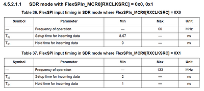
The following has been identified as limit to frequency when the internal loop-back (and not pin loop-back) is used:
Therefore if you need the GPIO you are in fact forced to reduce the QSPI clock frequency to ensure reliable operation.
Sorry about the slightly negative news....
Regards
Mark
uTasker project developer for Kinetis and i.MX RT]
Contact me by personal message or on the uTasker web site to discuss professional training or product development requirements
Thanks for the heads up @mjbcswitzerland
It's very frustrating when things like this are hidden away in the documentation, with almost zero chance of being spotted! Grrrrrrr........
-Nick
Hi Nick
I also modified my EVK 1060 reference and QSPI driver to not use the PAD loop-back method (which was also originally inherited from references that I had studied) and can confirm that all works normally.
#md 401f81e8 l 1
Memory Display
0x401f81e8 00000005 ....
shows that the default for this pin is in fact GPIO.
Therefore my conclusion is that the references unnecessarily use the PAD loop-back method for the standard QSPI flash devices and the internal loop-back is fine.
I have now modified my methods to only program the DQS pin and not use internal loop-back when the signal is really used externally - for example with HyperFlash (as is standard on the EVB 1050 boards).
This will also avoid users potentially having the same problem that you hit when the "seemingly" unused pin is configured.
Regards
Regards
Mark
uTasker project developer for Kinetis and i.MX RT]
I can be contacted by personal message or on the uTasker web site to discuss professional training or product development requirements, to accelerate progress or to solve technical problems

